Semiconductor device

a technology of semiconductor chips and semiconductors, applied in semiconductor devices, diodes, electrical equipment, etc., can solve the problems of mosfet breakage, high risk of short circuit generation, and fear of semiconductor chip breakage, so as to prevent short circuit generation, prevent corrosion of insulating films, and suppress threshold voltage reduction with time

Active Publication Date: 2012-05-31
MITSUBISHI ELECTRIC CORP
View PDF8 Cites 37 Cited by
  • Summary
  • Abstract
  • Description
  • Claims
  • Application Information

AI Technical Summary

Benefits of technology

[0009]It is an object of the present invention to provide a semiconductor device capable of suppressing reduction with time in a threshold voltage, preventing corrosion of an insulating film to be generated by an aluminum interconnect line, and preventing a short circuit to be generated between a gate and a source by Al spike.
[0010]The semiconductor device of the present invention includes: a main transistor cell with a polysilicon gate electrode formed on a semiconductor layer, and a source region that is an impurity region formed in an upper portion of the semiconductor layer; and an interlayer insulating film covering the gate electrode. A source electrode which contains aluminum and is connected to the source region extends on the interlayer insulating film. A gate pad containing aluminum is connected to the gate electrode. A barrier metal layer that prevents diffusion of aluminum is interposed between the source electrode and the interlayer insulating film, and between the gate pad and the gate electrode.
[0011]The barrier metal layer that prevents diffusion of aluminum is interposed between the source electrode and the interlayer insulating film, and between the gate pad and the gate electrode. This prevents reduction in a threshold voltage to be generated by voltage stress applied to the gate electrode of the transistor, thereby enhancing the stability of a MOSFET. Further, the interlayer insulating film is not corroded by Al contained in the source electrode and the gate pad, and Al spike is not generated in the polysilicon gate electrode even in a high-temperature condition, thereby preventing generation of a short circuit between the gate and the source.

Problems solved by technology

Reduction in the threshold voltage increases the transfer characteristics (ratio of output to input) of the MOSFET to generate flow of overcurrent during the actual use of the MOSFET, resulting in a fear of breakage of the MOSFET.
This generates nonuniformity of the operations of a plurality of MOSFET cells of a semiconductor chip, resulting in a fear of breakage of the semiconductor chip.
Further, even if no problem in electric characteristics is found as a result of the test, the threshold voltage may be reduced due to prolonged application of voltage stress between the gate and the source, so the aforementioned problem is likely to occur.
Meanwhile, Al forming a source electrode may cause corrosion of an interlayer insulating film intended to maintain the isolation between the gate and the source, or may diffuse into polysilicon forming a gate interconnect line that is what is called “Al spike,” resulting in a fear of formation of a short circuit between the gate and the source.

Method used


Image

  • Semiconductor device
  • Semiconductor device
  • Semiconductor device

Examples


first preferred embodiment

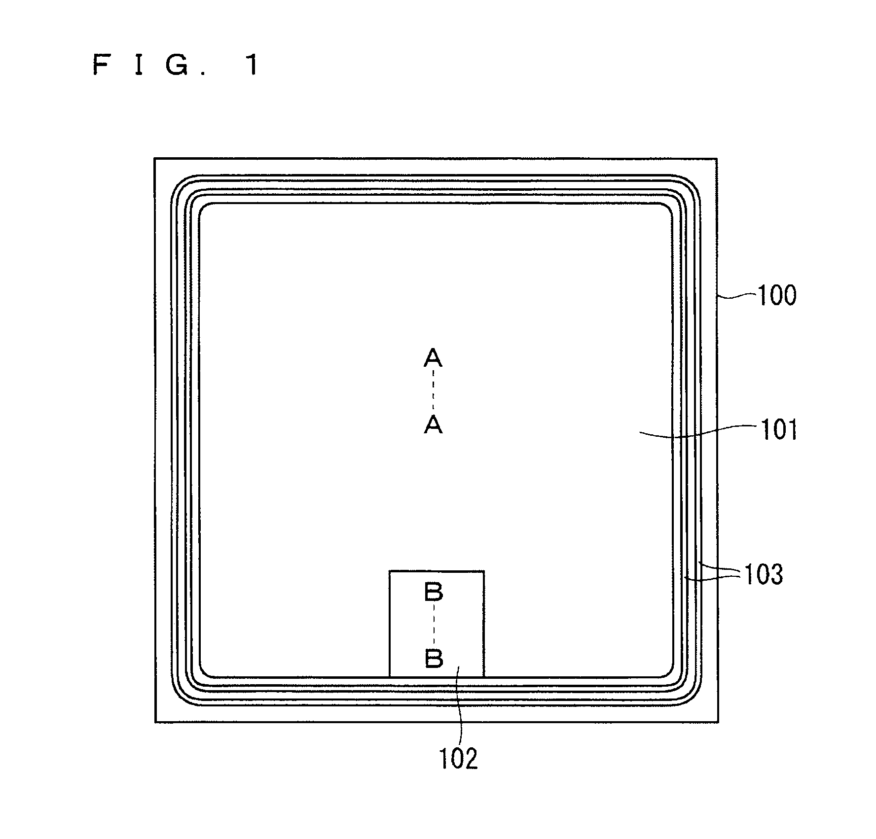
[0028]FIG. 1 is a top view of a semiconductor chip with a semiconductor device of a first preferred embodiment of the present invention. An SiC-MOSFET is shown as an example of the semiconductor device. A source electrode 101 and a gate pad 102 connected to a gate electrode are formed on the upper surface of a MOSFET chip 100 to hold the MOSFET. A field limiting ring 103 is provided as a termination structure on the outer circumference of the MOSFET chip 100.

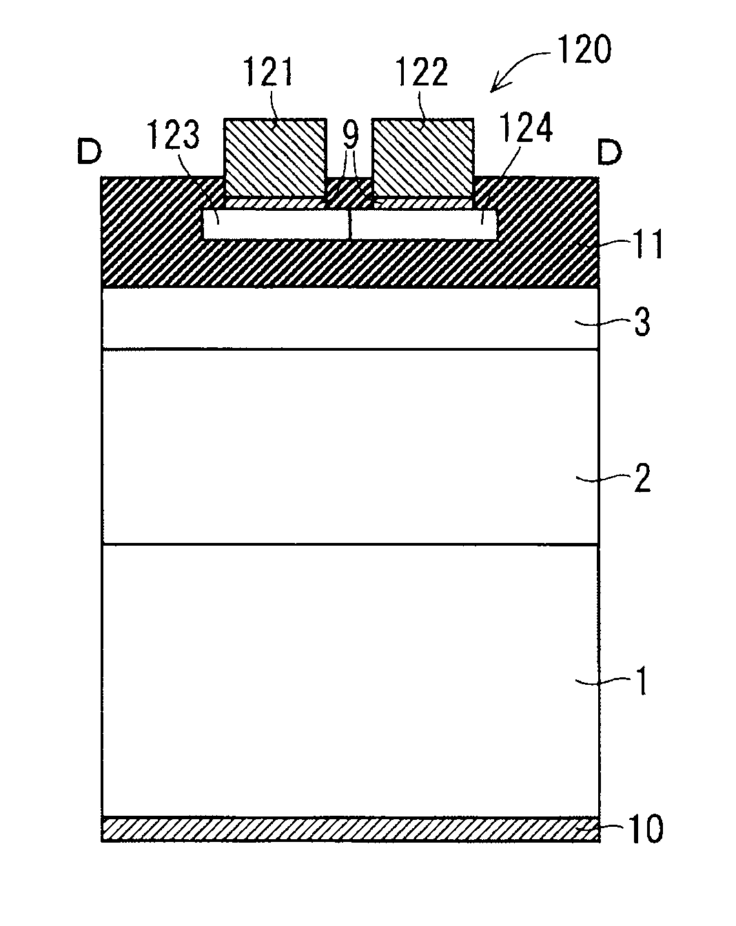
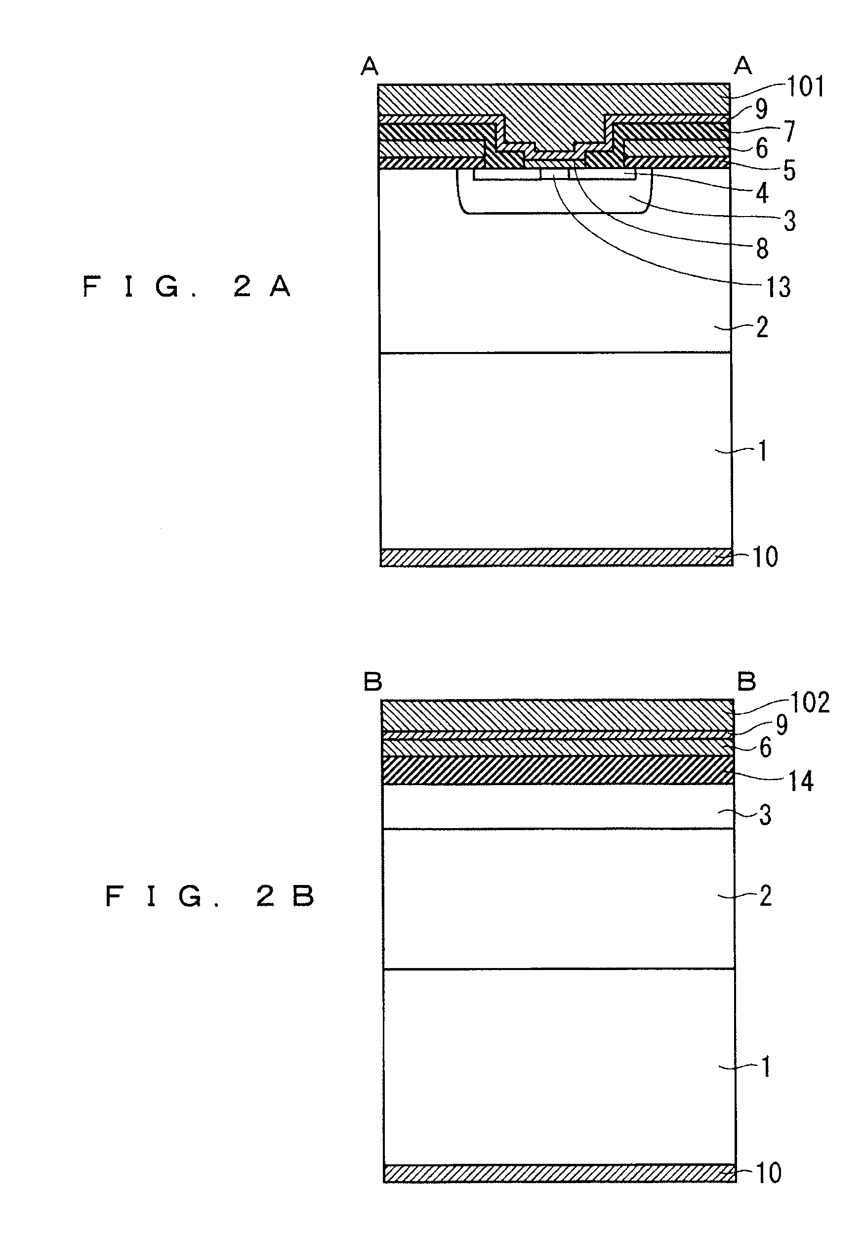
[0029]FIGS. 2A and 2B are sectional views of the MOSFET chip 100. FIG. 2A is a sectional view of a MOSFET cell portion (cross section taken along a line A-A of FIG. 1). FIG. 2B is a sectional view of a gate pad portion (cross section taken along a line B-B of FIG. 1). The MOSFET chip 100 includes parallel connection of a plurality of cells of the structure shown in FIG. 2A, and the gate electrode of each of the cells is connected to the gate pad 102.

[0030]The MOSFET includes an SiC substrate to become an n+-buffer layer 1, and a...

second preferred embodiment

[0040]Some MOSFETs include a current sensing cell that detects current flowing in the MOSFETs. An exemplary object of the current sensing cell is to detect overcurrent so that the MOSFETs can be protected from breakage due to overcurrent. The current sensing cell generally shares a gate and a drain with a MOSFET cell normally used (main MOSFET cell). The current sensing cell diverts part of main current flowing in a MOSFET to obtain minute current that is in proportion to the main current.

[0041]FIG. 6 is a top view of a MOSFET chip 100 of a second preferred embodiment. Some of MOSFET cells of the MOSFET chip 100 is used as a current sensing cell 110. A source electrode (current sensing electrode) 111 of the current sensing cell 110 is separated from a source electrode 101 of a main MOSFET cell, whereas the gate electrode of the current sensing cell 110 is shared with the main MOSFET cell and is connected to a gate pad 102.

[0042]FIG. 7 is a sectional view of the current sensing cell ...

third preferred embodiment

[0046]It has been derived from the first preferred embodiment that the thickness of the barrier metal layer 9 of 60 nm or more can limit reduction of a threshold voltage to be about 0.2 V or less from the results (FIG. 4) of the HTGB test conducted in the cases where the barrier metal layer 9 had a thickness of 30 nm and 75 nm.

[0047]However, the inventors have conducted further experiments and found that the effect of suppressing reduction of a threshold voltage has already become saturated in the state in which the thickness of the Ti barrier metal layer 9 is smaller than 75 nm and reduction of a threshold voltage can be suppressed sufficiently even in a case where the thickness of the barrier metal layer 9 is smaller than 60 nm. The experimental results thereof are described below.

[0048]FIG. 8 shows a relationship between the thickness of the Ti barrier metal layer 9 and the change of the threshold voltage (VGSth) of the MOSFET. Here, the HTGB test similar to that of FIG. 3 was co...


PUM


Abstract

A MOSFET cell of a semiconductor device includes a polysilicon gate electrode and an n+-source region formed in an upper portion of an n−-drift layer. An interlayer insulating film covers the gate electrode. An Al source electrode extends on the interlayer insulating film. An Al gate pad is connected to the gate electrode. A barrier metal layer that prevents diffusion of aluminum is interposed between the source electrode and the interlayer insulating film, and between the gate pad and the gate electrode.

Description

BACKGROUND OF THE INVENTION[0001]1. Field of the Invention[0002]The present invention relates to a semiconductor device, and more specifically to a semiconductor device with a transistor cell with a polysilicon gate electrode and an interconnect line containing aluminum.[0003]2. Description of the Background Art[0004]Semiconductor elements (MOSFETs (metal oxide semiconductor field effect transistors), IGBTs (insulated gate bipolar transistors) and others) formed by using silicon carbide (SiC) are promising candidates for next-generation switching elements capable of achieving high breakdown voltage, low loss, and high resistance to heat, and are expected to be applied to power semiconductor devices such as inverters.[0005]A generally employed structure of a conventional MOSFET using SiC (SiC-MOSFET) is such that a silicide layer to make ohmic contact is formed on a source region, and a source electrode made of aluminum (Al) is formed on the silicide layer (see for example Japanese P...

Claims


Application Information

Patent Timeline
Patent Type & Authority Applications(United States)
IPC IPC(8): H01L29/04H01L29/12
CPCH01L29/1608H01L29/45H01L29/4941H01L29/861H01L29/7804H01L29/7815H01L29/7802H01L29/7811H01L2224/0603H01L21/18H01L29/772H01L29/456H01L29/78
Inventor SUEKAWA, EISUKEORITSUKI, YASUNORITARUI, YOICHIRO
Owner MITSUBISHI ELECTRIC CORP
Why Eureka
Try Eureka