SOI SiGe-Base Lateral Bipolar Junction Transistor

a lateral bipolar junction and transistor technology, applied in the field of lateral bipolar transistors, can solve the problems of performance limiting factors for bipolar junctions, noise generated at the periphery of the base is another performance limiting factor, and the capacitance between the extrinsic base, so as to minimize the introduction of noise, reduce the effect of parasitic capacitance and increase current density

Active Publication Date: 2012-06-07
IBM CORP
View PDF7 Cites 319 Cited by
  • Summary
  • Abstract
  • Description
  • Claims
  • Application Information

AI Technical Summary

Benefits of technology

[0004]A lateral heterojunction bipolar transistor (HBT) is formed on a semiconductor-on-insulator substrate. The HBT includes a base including a doped silicon-germanium alloy base region, an emitter including doped silicon and laterally contacting the base, and a collector including doped silicon and laterally contacting the base. Because the collector current is channeled through the doped silicon-germanium base region having a band gap less than silicon, the HBT can accommodate a greater current density at a given emitter-base forward bias voltage than a comparable bipolar transistor employing a silicon base region. The base may also include an upper silicon base region and / or a lower silicon base region. In this case, the collector current is concentrated in the doped silicon-germanium base region, thereby minimizing noise introduced to carrier scattering at the periphery of the base. Further, parasitic capacitance is minimized because the emitter-base junction area is the same as the collector-base junction area.

Problems solved by technology

The parasitic capacitance between the extrinsic base, the emitter, and / or the collector is a performance-limiting factor for a bipolar junction transistor.
The noise generated at the periphery of the base is another performance-limiting factor for a bipolar junction transistor.
Yet another performance-limiting factor for a bipolar junction transistor is the maximum current density that the transistor can handle without speed degradation.
While many types of bipolar junction transistors have been proposed in the prior art, most fail to simultaneously address the above issues, let alone providing a satisfactory solution addressing them.

Method used


Image

  • SOI SiGe-Base Lateral Bipolar Junction Transistor
  • SOI SiGe-Base Lateral Bipolar Junction Transistor
  • SOI SiGe-Base Lateral Bipolar Junction Transistor

Examples


first embodiment

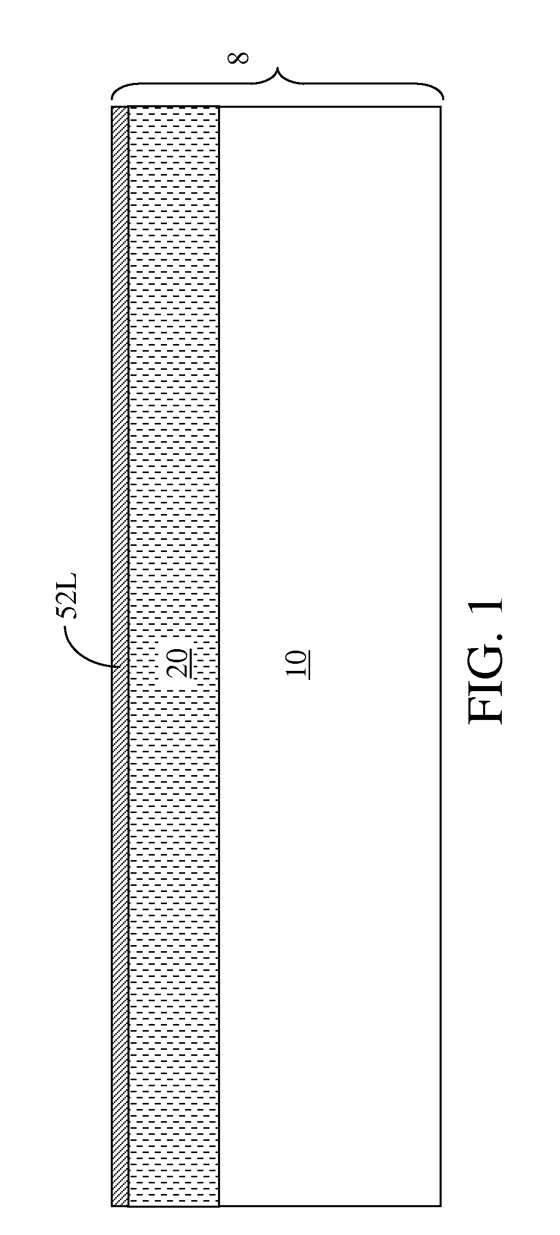
[0022]Referring to FIG. 1, a first exemplary semiconductor structure according to the present disclosure includes a substrate 8 including at least a dielectric material layer and a silicon layer located on a top surface of the dielectric material layer. The substrate 8 can be, for example, a semiconductor-on-insulator (SOI) substrate, which includes a handle substrate 10, a buried insulator layer 20 contacting a top surface of the handle substrate 10, and a silicon layer contacting a top surface of the buried insulator layer 20. This silicon layer is herein referred to as a lower silicon layer 52L because another silicon layer can be subsequently formed over the lower silicon layer 52L.

[0023]The handle substrate 10 can include a semiconductor material, an insulator material, a conductor material, or a combination thereof. In one example, the handle substrate 10 can include a semiconductor material such as silicon. If the handle substrate 10 includes a semiconductor material, the han...

second embodiment

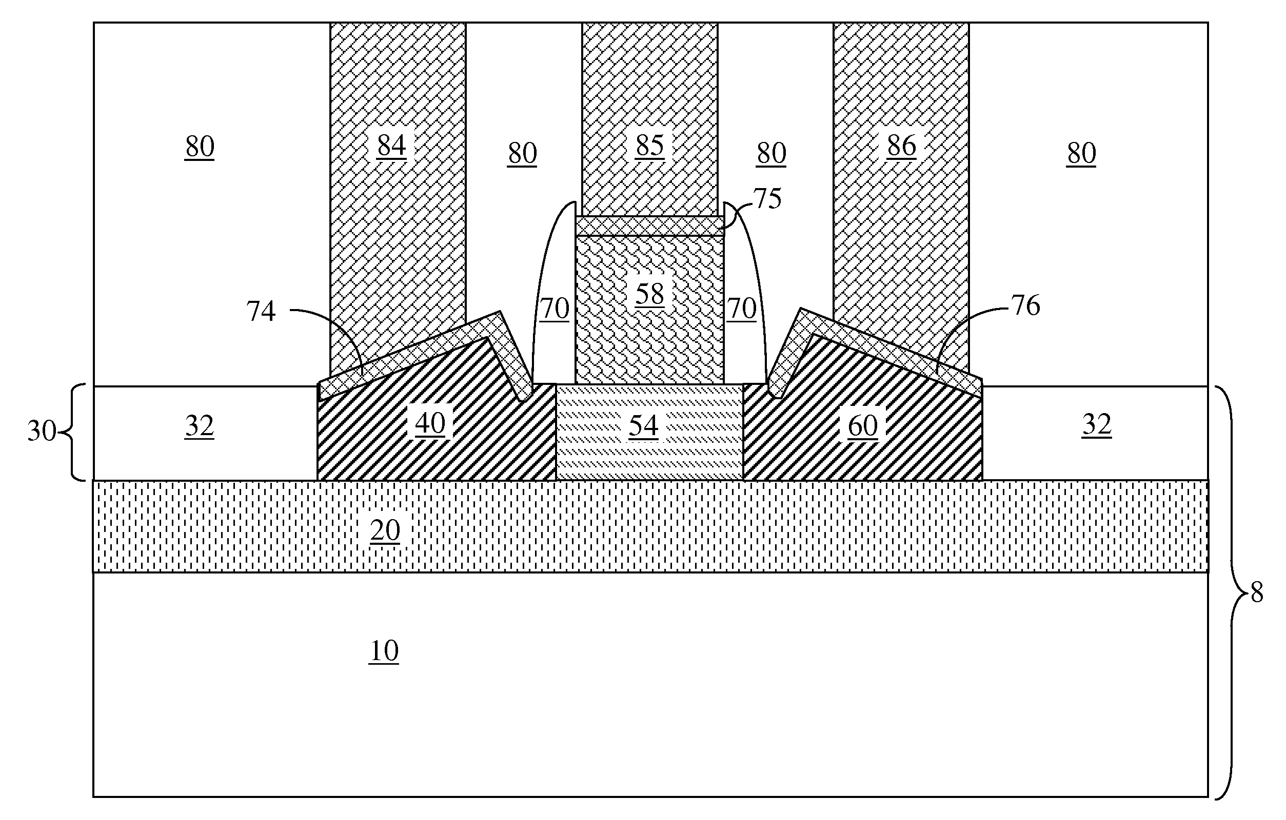
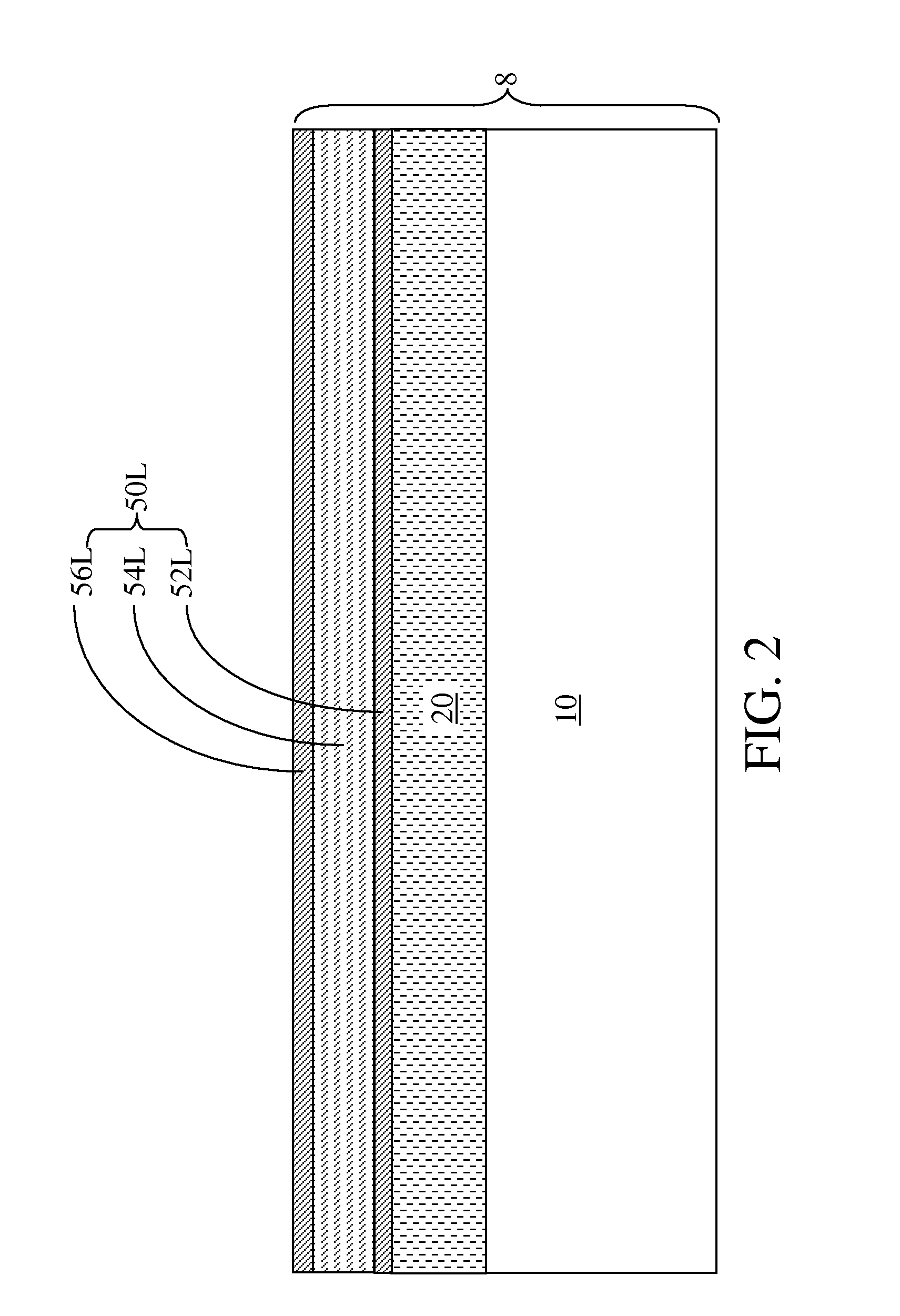
[0056]Referring to FIG. 10, a second exemplary semiconductors structure according to the present disclosure can be derived from the first exemplary semiconductor structure shown in FIG. 7 by omitting the formation of the upper silicon layer 56L at a processing step corresponding to FIG. 2. As a consequence, an upper silicon base region is not formed in the second exemplary semiconductor structure, and the base 50 includes only a lower silicon base region 52 and a silicon-germanium base region 54. The silicon-germanium base region 54 contacts the bottom surfaces of the extrinsic base 58 and the dielectric spacer 70.

[0057]Referring to FIG. 11, a variation of the second exemplary semiconductors structure can be derived from the variation of the first exemplary semiconductor structure as shown in FIG. 9 by omitting the formation of the upper silicon layer 56L at a processing step corresponding to FIG. 2. As a consequence, an upper silicon base region is not formed in the variation of th...

fourth embodiment

[0062]Referring to FIG. 14, a fourth exemplary semiconductor structure according to the present disclosure is derived from the third exemplary semiconductor structure of FIG. 13 by omitting formation of the upper silicon layer 56L. In the fourth exemplary semiconductor structure, the base 50 consists of the silicon-germanium base region 54. The silicon-germanium base region 54 has a doping of the first conductivity type, and contacts a top surface of the buried insulator layer 20, the emitter 40, the collector 60, and a bottom surface of the extrinsic base 58. A first heterojunction is formed between the emitter 40 and the base 50, and a second heterojunction is formed between the base 50 and the collector.

[0063]In each of the exemplary semiconductor structures illustrated above, the collector current flows primarily in and through a silicon-germanium alloy region, i.e., the silicon-germanium base region 54, which has a smaller band gap than silicon regions, i.e., the upper silicon ...


PUM

PropertyMeasurementUnit
thicknessesaaaaaaaaaa

Abstract

A lateral heterojunction bipolar transistor (HBT) is formed on a semiconductor-on-insulator substrate. The HBT includes a base including a doped silicon-germanium alloy base region, an emitter including doped silicon and laterally contacting the base, and a collector including doped silicon and laterally contacting the base. Because the collector current is channeled through the doped silicon-germanium base region, the HBT can accommodate a greater current density than a comparable bipolar transistor employing a silicon channel. The base may also include an upper silicon base region and / or a lower silicon base region. In this case, the collector current is concentrated in the doped silicon-germanium base region, thereby minimizing noise introduced to carrier scattering at the periphery of the base. Further, parasitic capacitance is minimized because the emitter-base junction area is the same as the collector-base junction area.

Description

BACKGROUND[0001]The present disclosure relates to a lateral bipolar transistor (BJT) structure, and particularly to a lateral bipolar junction transistor including a SiGe base and located on an semiconductor-on-insulator (SOI) substrate and methods of manufacturing the same.[0002]The parasitic capacitance between the extrinsic base, the emitter, and / or the collector is a performance-limiting factor for a bipolar junction transistor. The parasitic capacitance reduces the switching speed of the bipolar junction transistor. The noise generated at the periphery of the base is another performance-limiting factor for a bipolar junction transistor. Typically, charge carriers can be temporarily captured at an interface between the base and a surrounding dielectric material, and emitted at a subsequent time to introduce electrical noise in the signal. In order to provide signal amplification with high fidelity, such noise must be suppressed to a minimum level. Yet another performance-limitin...

Claims


Application Information

Patent Timeline
Patent Type & Authority Applications(United States)
IPC IPC(8): H01L29/737H01L21/8222
CPCH01L27/0821H01L27/1203H01L29/7317H01L29/165H01L29/66265H01L29/0808
Inventor NING, TAK H.CHAN, KEVIN K.KHATER, MARWAN H.
Owner IBM CORP
Why Eureka
Try Eureka