Pre-bonded substrate for integrated circuit package and method of making the same
- Summary
- Abstract
- Description
- Claims
- Application Information
AI Technical Summary
Benefits of technology
Problems solved by technology
Method used
Image
Examples
first embodiment
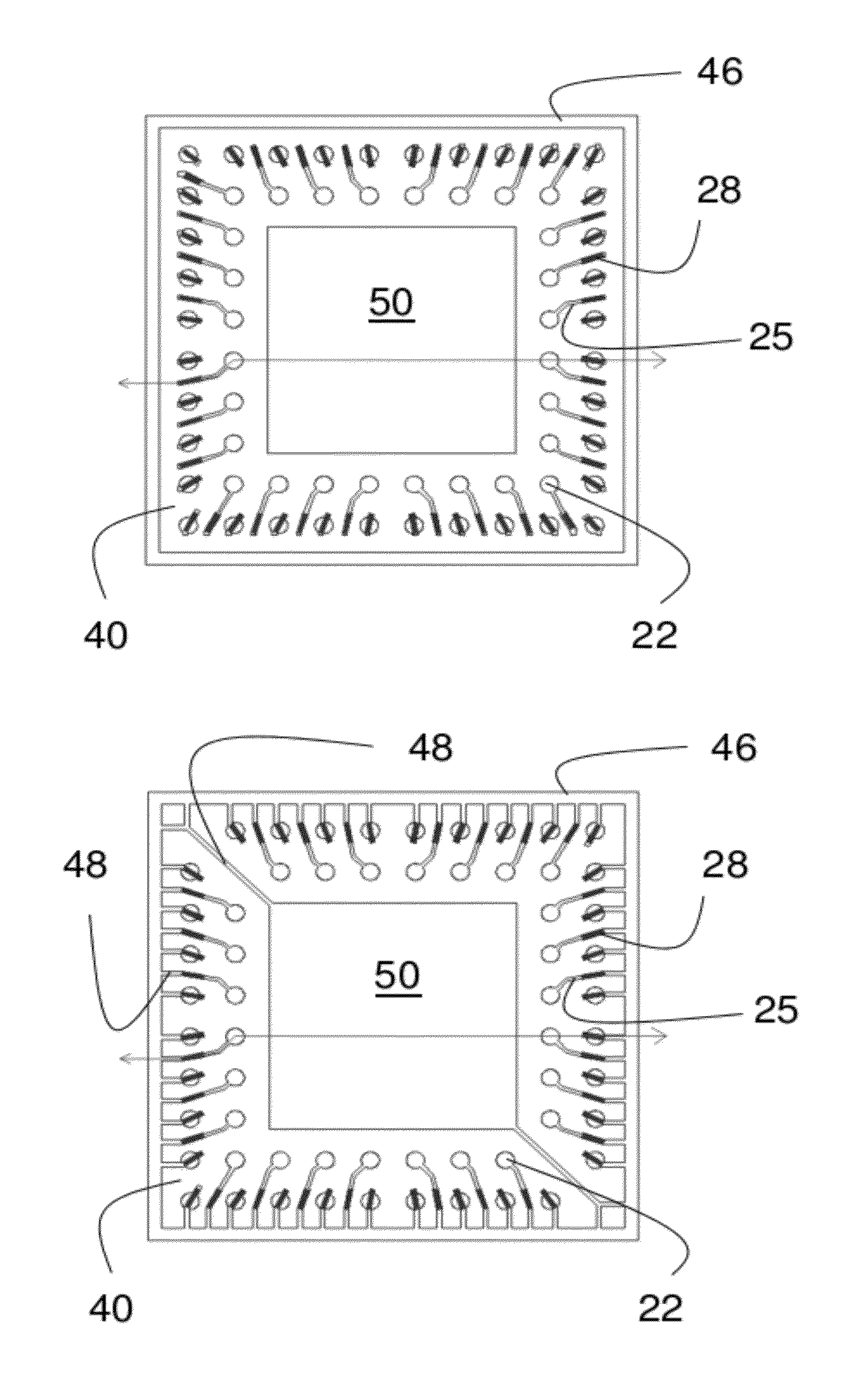
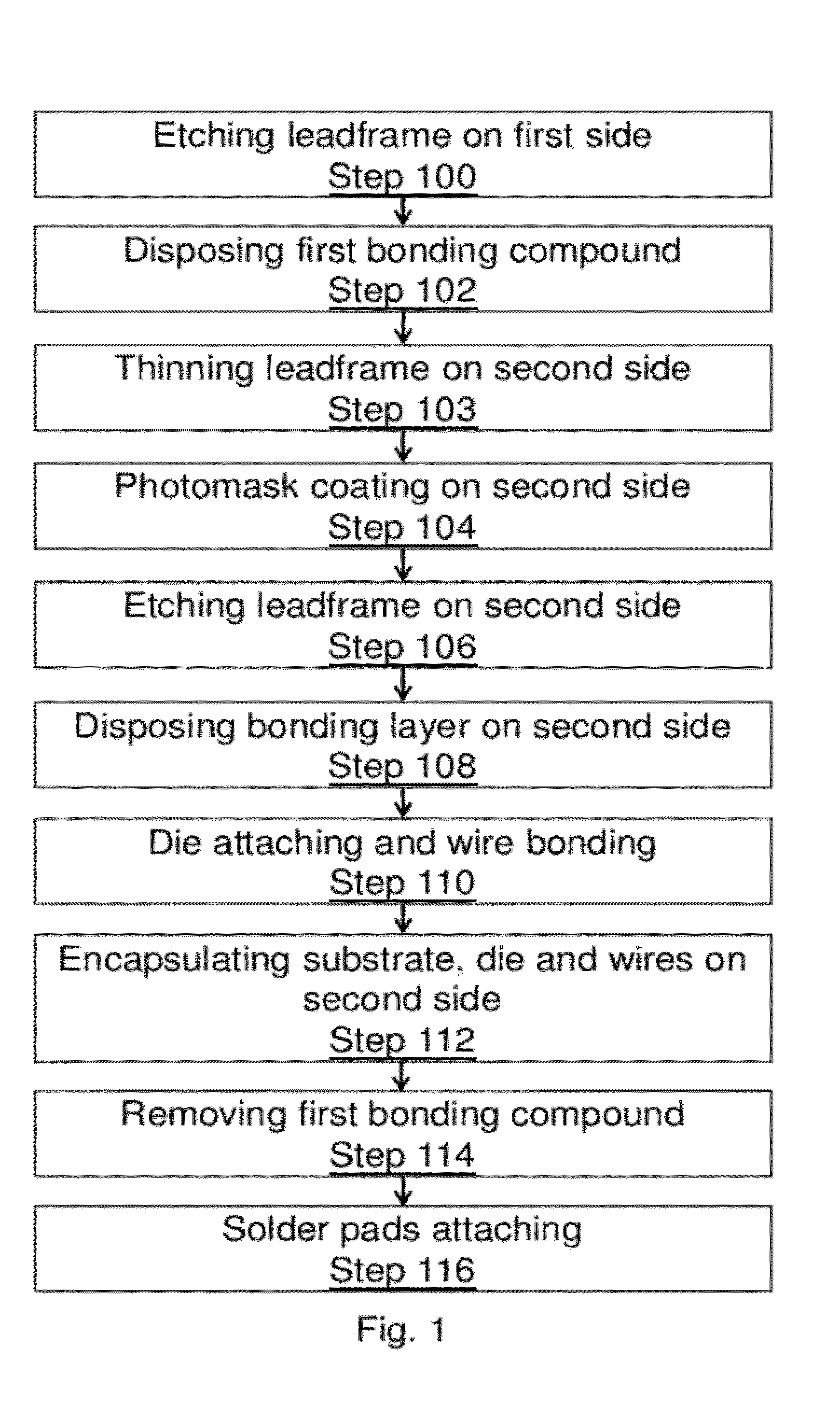
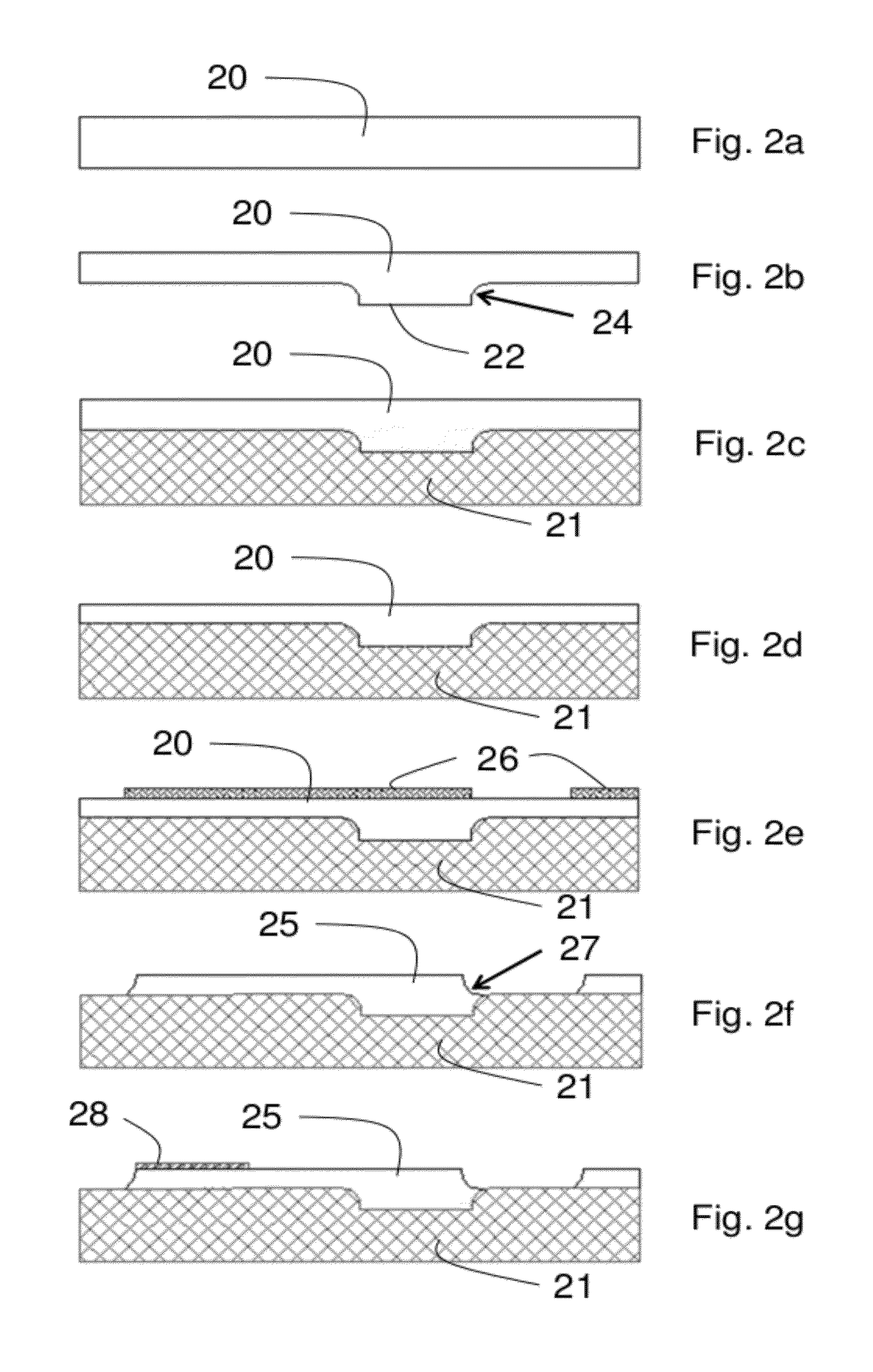
[0040]FIGS. 1 and 2a-2h shows a method of manufacturing a substrate and an IC package according to the present invention. FIG. 2a shows an electrically conductive substrate leadframe 20, made from copper for example, at its initial state. In step 100, a first portion of the leadframe 20 is etched at a first side thereof to form a first pattern on the first side. The first pattern comprises a plurality of lands 22 on the surface of the first side, adapted to electrically connect to an external device, such as a printed circuit board, and also comprises a first recessed portion 24 which is recessed relative to the plurality of lands 22. The first pattern can alternately be called as the landing pattern. The substrate after step 100 is shown in FIG. 2b.
[0041]In step 102, a first bonding compound 21 is disposed on the first side of the leadframe 20. The bonding compound 21 fills the first recessed portion 24 and also covers the plurality of lands 22. In an exemplary embodiment, the fir...
second embodiment
[0050]In the present invention as shown in FIGS. 3 and 4a-4k, the leadframe 20 is first etched at the first side (step 200), then the first bonding compound 21 is disposed on the first side (step 202), and the optional thinning step is performed (step 203). In this embodiment, the bonding layer is then disposed (step 204) before coating the photomask 26 (step 206) and etching the leadframe on the second side to reveal the routing leads 25 (step 208). That means the bonding layer is first disposed on the leadframe 20 at the second side, then the photomask 26 is disposed on the leadframe 20 at the second side, covering the routing leads 25 as well as the bonding pads 28, as shown in FIG. 4f. The semiconductor die 30 is then attached with wire bonding (step 210), the encapsulation compound 34 is disposed (step 212), the first bonding compound 21 is selectively removed from the first side (step 214), and solder pads 36 are disposed on the lands 22 (step 216). The substrate or IC package...
PUM
 Abstract
Description
Claims
Application Information


