Semiconductor package and fabrication method thereof

a technology of semiconductor and packaging, applied in the direction of semiconductor/solid-state device details, semiconductor devices, electrical apparatus, etc., can solve the problems of excessive via density in semiconductor systems, defect in final products, and reduced distance between neighboring vias and via diameter, so as to enhance the reliability of wafer level molding and wafer level packaging process, the effect of reducing stress

Inactive Publication Date: 2012-06-14
NEPES CO LTD
View PDF3 Cites 37 Cited by
  • Summary
  • Abstract
  • Description
  • Claims
  • Application Information

AI Technical Summary

Benefits of technology

[0006]Therefore, the present invention is directed to provide a new semiconductor package with enhanced reliability and performance.
[0007]Another object of the present invention is to provide a semiconductor package with a new package substrate having a via set therein.Still another object of the present invention is to provide a semiconductor packaging process with enhanced reliability and effectiveness.
[0015]According to the present invention, by minimizing the volume of the conductive material filled in the vertical through hole of a package substrate, the present invention can relieve the stress between the different materials in packaging process, and enhances the reliability of wafer level molding and wafer level packaging process.
[0016]Moreover, the present invention allows high degree of freedom of material and layout in semiconductor package such that excellent devices can be fabricated in wafer level metallization and molding process.Furthermore, the present invention improves durability and electrical performance of a semiconductor package, and allows cost effectiveness and high yield in semiconductor packaging process.

Problems solved by technology

However, through-via technology has to solve some technical problems that the distance between neighboring vias and via diameter should be reduced for a high integrated semiconductor chip.
Another technical issue relates to excessive via density in a semiconductor system.
A package substrate with a lot of vias therein suffers from thermal stress between a semiconductor substrate and via filling material in fabrication process.
The thermal stress leads to defects in final product and difficulties in following process.
Moreover, due to a lot of vias, the package substrate has increased volume of conductive material therein, which results in deterioration of electrical and mechanical reliability of a semiconductor package.

Method used


Image

  • Semiconductor package and fabrication method thereof
  • Semiconductor package and fabrication method thereof
  • Semiconductor package and fabrication method thereof

Examples


first embodiment

[0042]The semiconductor package of the present invention can be fabricated in two different processes, according to the order of via set formation, front side process, back side process, carrier bonding, semiconductor chip mounting, and molding layer formation. Referring to FIGS. 7 to 10, the fabrication process in accordance with the present invention will be described.

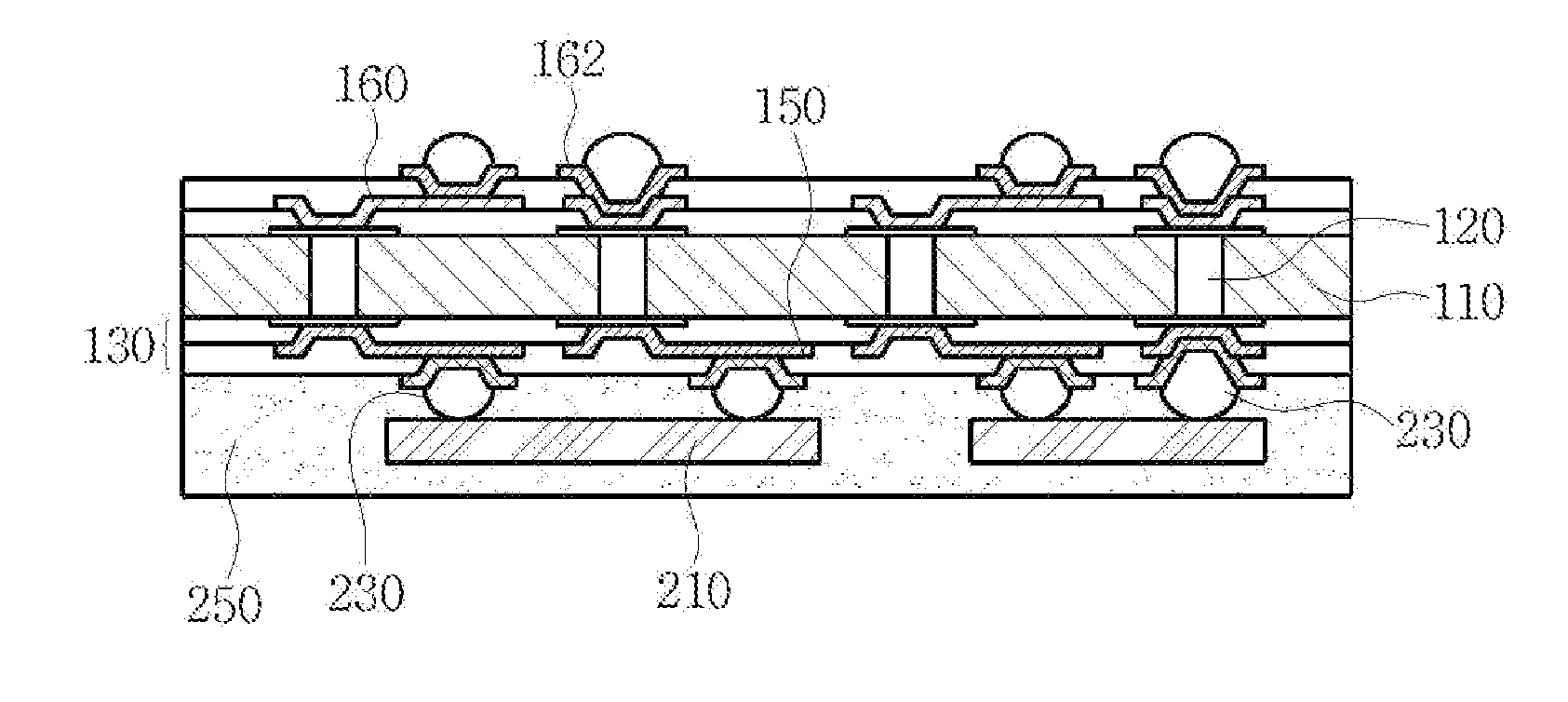
[0043]Firstly, a package substrate (110) is prepared. The substrate (110) has a first surface and a second surface in the opposite side. The package substrate is partially etched to form a plurality of via sets (120). The via sets can be formed by physical method such as laser etching and RIE, or chemical method such as wet etching. Conductive material is filled up in the via set by such as electroplating. The via set is necessarily to completely perforate the package substrate, and can be formed in predetermined depth considering the thickness of the final package substrate.

[0044]Next, a back side process is perform...

second embodiment

[0048]Now, the fabrication process in accordance with the present invention will be described. In this embodiment, the front side process, semiconductor chip mounting and wafer level molding process are performed prior to the back side process.

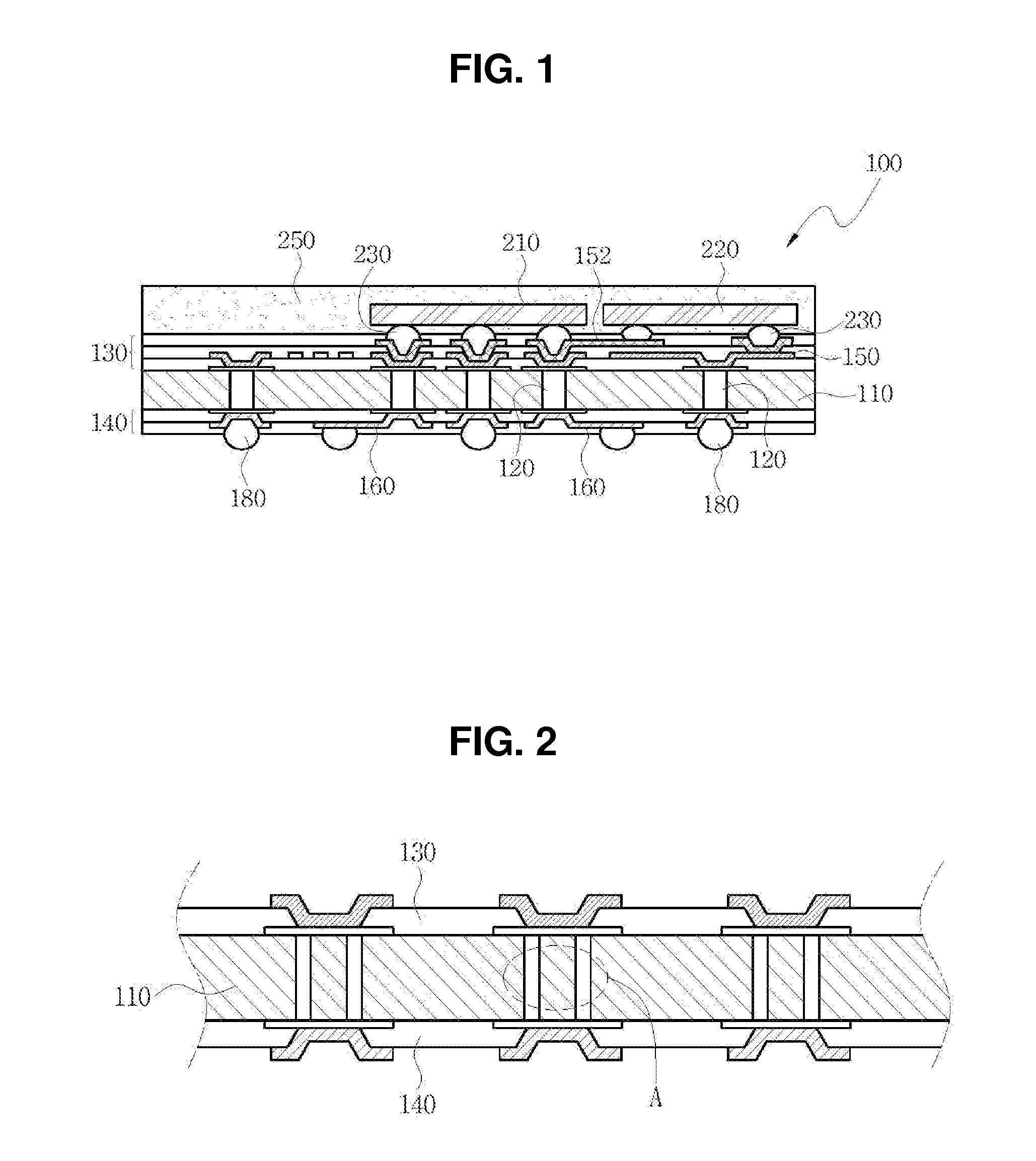
[0049]Firstly, as shown in FIG. 11, a plurality of via sets (120) is formed in a package substrate (110) and conductive material is filled up in the via set. During the front side process, a first dielectric layer (130) and a first redistribution layer (150) are formed on the first surface of the package substrate. Then, a semiconductor chip (210) is mounted over the package substrate to be electrically connected the first redistribution layer, and a molding layer (250) is formed in wafer level to cover the semiconductor chip.

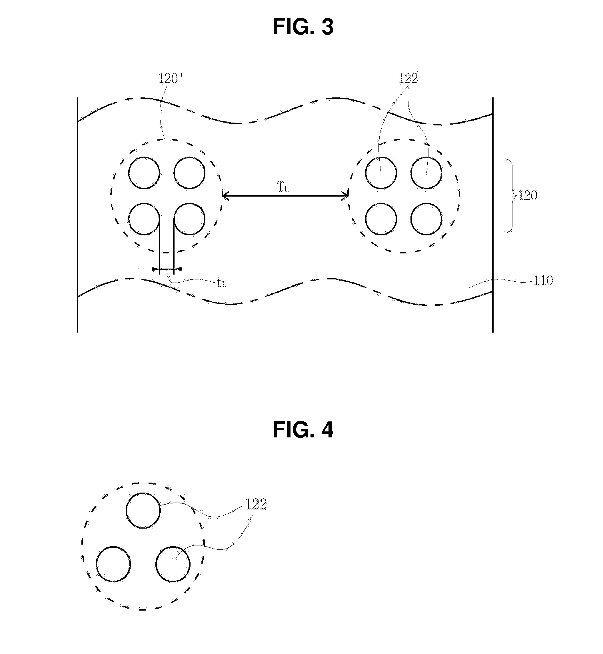
[0050]In wafer level process, excessive via density in a package substrate makes worse the thermal stress between the molding layer and the package substrate such that the following processes may be difficult to be contin...


PUM


Abstract

A semiconductor package is provided. The package includes a package substrate with a first surface and a second surface on the opposite side, and a plurality of via sets connecting vertically the first surface with the second surface, said via sets having a plurality of micro vias and filled with conductive material. The micro vias are grouped together, and the distance between micro vias in the via set is smaller than the distance between neighboring via sets.

Description

TECHNICAL FIELD[0001]The present invention relates to a semiconductor package, and more particularly, to a new semiconductor package with a package substrate having via sets therein.BACKGROUND ART[0002]As personal computers, portable phones, personal information terminals and electronic products have become small, light and been functionalized, data processing capacity has greatly increased. In accordance with this tendency, a wafer level chip size package has been considered as suitable technology for small sized and high speed package. Development of integration technology and new electronic devices requires enhanced semiconductor system with high performance. Semiconductor system such as SiP includes plurality of semiconductor chips and other electronic components in a single package. To efficiently fabricate semiconductor systems, various high technologies related to chip integration, metallization layout, or stacking are required.[0003]As the size of a chip gets smaller, a semi...

Claims


Application Information

Patent Timeline
Patent Type & Authority Applications(United States)
IPC IPC(8): H01L23/485H01L21/50H01L23/48H01L21/56
CPCH01L21/486H01L23/147H01L23/3128H01L23/49827H01L24/16H01L2924/00013H01L2924/15311H01L2224/16237H01L2924/01005H01L2924/01033H01L2924/01029H01L2224/13099H01L2224/13599H01L2224/05599H01L2224/05099H01L2224/29099H01L2224/29599H01L2924/14H01L2924/351
Inventor KANG, IN SOOKWON, YONG TAEPARK, BYUNG JIN
Owner NEPES CO LTD
Why Eureka
Try Eureka