Semiconductor memory devices, memory systems and methods of operating semiconductor memory devices

a memory device and semiconductor technology, applied in the field of memory, can solve the problems of reducing the yield of the dram, increasing the bit errors of the memory cells in the dram, and achieving the effect of improving reliability and performan

Active Publication Date: 2018-12-13
SAMSUNG ELECTRONICS CO LTD
View PDF6 Cites 3 Cited by
  • Summary
  • Abstract
  • Description
  • Claims
  • Application Information

AI Technical Summary

Benefits of technology

[0005]At least one exemplary embodiment of the inventive concept may provid

Problems solved by technology

However, due to the continuing shrink in the fabrication design rule of DRAMs, bit error

Method used


Image

  • Semiconductor memory devices, memory systems and methods of operating semiconductor memory devices
  • Semiconductor memory devices, memory systems and methods of operating semiconductor memory devices
  • Semiconductor memory devices, memory systems and methods of operating semiconductor memory devices

Examples


Embodiment Construction

[0035]The inventive concept will be described more fully hereinafter with reference to the accompanying drawings, in which exemplary embodiments thereof are shown.

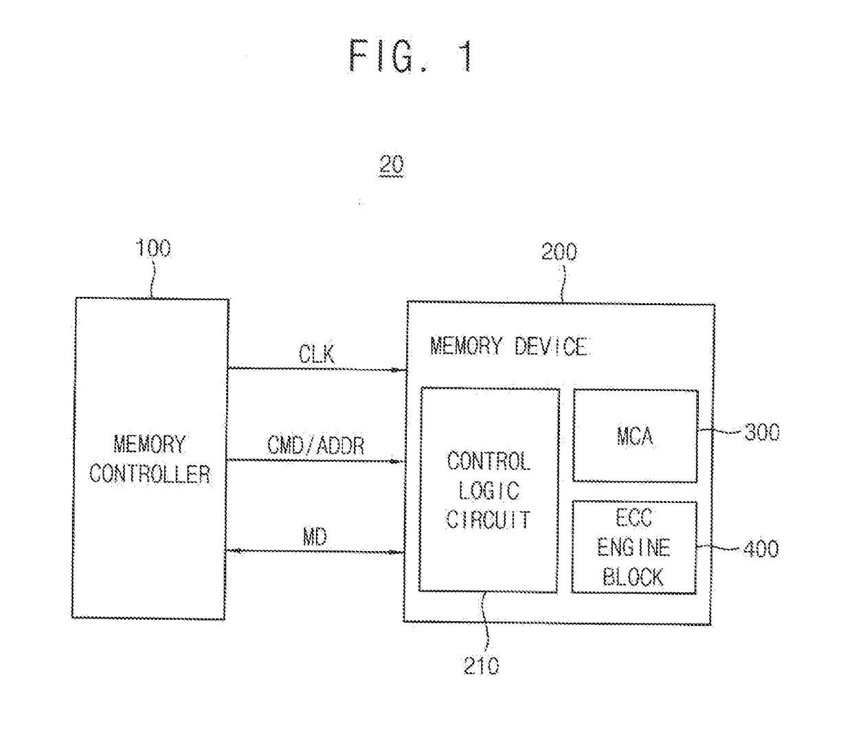
[0036]FIG. 1 is a block diagram illustrating a memory system according to an exemplary embodiment of the inventive concept.

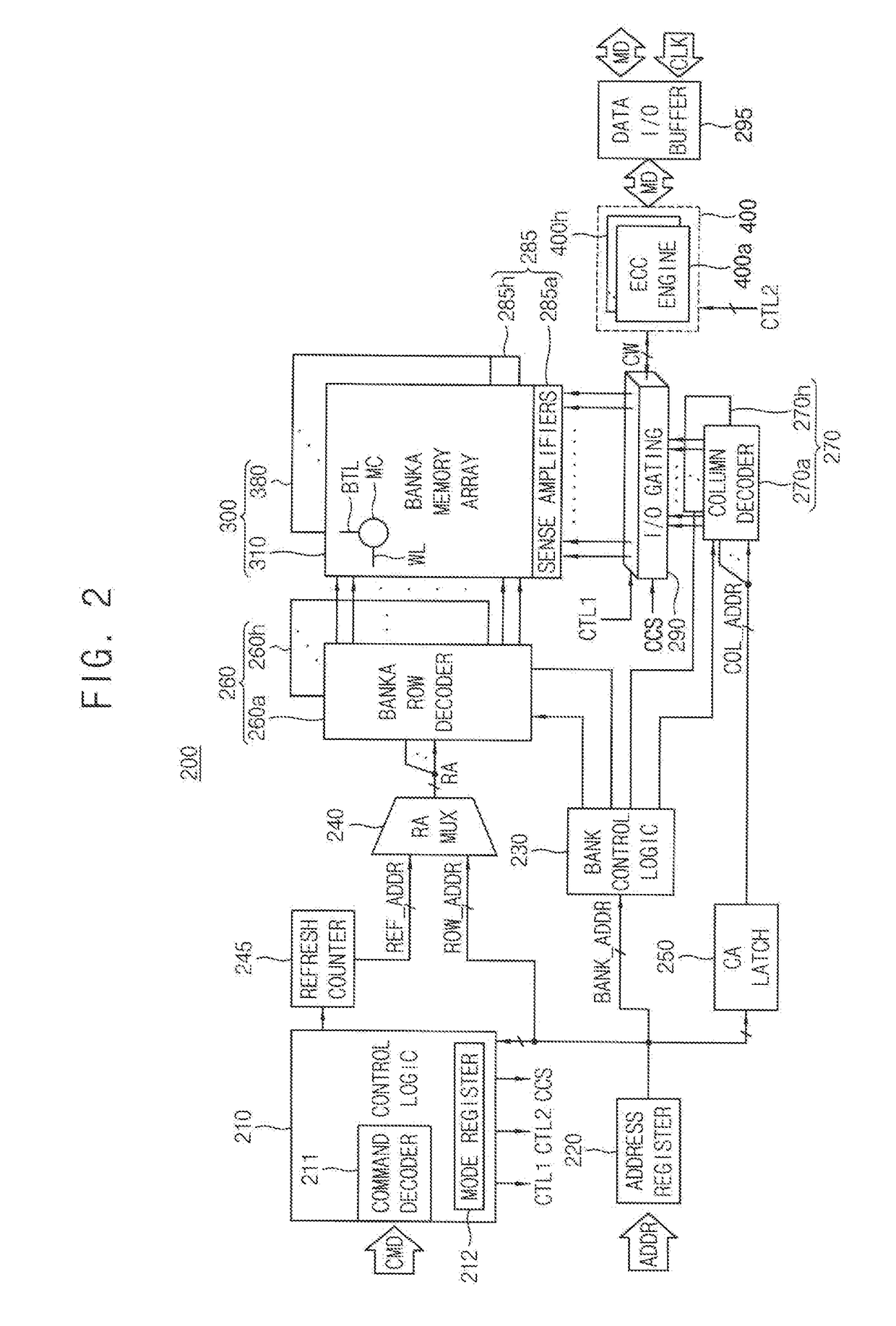
[0037]Referring to FIG. 1, a memory system 20 includes a memory controller 100 and a semiconductor memory device 200.

[0038]The memory controller 100 may control an overall operation of the memory system 20. The memory controller 100 may control an overall data exchange between an external host and the semiconductor memory device 200. For example, the memory controller 100 may write data in the semiconductor memory device 200 or read data from the semiconductor memory device 200 in response to a request from the host. The request may be sent as a message from the host to the semiconductor memory device 200.

[0039]In addition, the memory controller 100 may issue operation commands to the semiconductor mem...


PUM


Abstract

A semiconductor memory device includes a memory cell array, an error correction code (ECC) engine, an input/output (I/O) gating circuit and a control logic circuit. The memory cell array includes bank arrays, each of the bank arrays includes a first sub array and a second sub array, and each of the first sub array and the second sub array includes a normal cell region to store data bits and a parity cell region to store parity bits. The ECC engine generates the parity bits and corrects error bit. The I/O gating circuit is connected between the ECC engine and the memory cell array. The control logic circuit controls the I/O gating circuit to perform column access to the normal cell region according to a multiple of a burst length and to perform column access to the parity cell region according to a non-multiple of the burst length partially.

Description

CROSS-REFERENCE TO RELATED APPLICATIONS[0001]This US application claims the benefit of priority under 35 USC § 119 to Korean Patent Application No. 10-2017-0072223, filed on Jun. 9, 2017, in the Korean Intellectual Property Office, the disclosure of which is incorporated by reference in its entirety herein.BACKGROUND1. Technical Field[0002]The present disclosure relates to memories, and more particularly to semiconductor memory devices, memory systems and methods of operating semiconductor memory devices.2. Discussion of Related Art[0003]Semiconductor memory devices may be classified into non-volatile memory devices such as flash memory devices and volatile memory devices such as dynamic random access memories (DRAMs). A non-volatile memory can retrieve stored information even after its power supply has been removed and a volatile memory needs constant power to prevent its data from being erased.[0004]High speed operation and cost efficiency of DRAMs make it possible for DRAMs to be...

Claims


Application Information

Patent Timeline
IPC IPC(8): G11C7/10G11C11/4093G11C11/4096G06F11/10H03M13/00
CPCG11C7/1006G11C11/4093G11C11/4096G11C7/106G11C7/1087G06F11/1044H03M13/611G11C29/42G11C7/1018G11C29/52G11C2029/0411G06F11/1048H03M13/05
Inventor CHA, SANG-UHNSEO, YOUNG -HUNPARK, KWANG-ILBAE, SEUNG-JUN
Owner SAMSUNG ELECTRONICS CO LTD
Why Eureka
Try Eureka