Control-voltage of pass-gate follows signal

a control voltage and passgate technology, applied in the direction of pulse automatic control, pulse technique, electronic switching, etc., can solve the problems of capacitive load, device cannot withstand large voltages across their terminals, and the on-resistance of supply voltage and level, so as to improve the higher-frequency common-mode tracking of control voltage, the effect of low power consumption and high impedan

Active Publication Date: 2012-06-14
NXP BV
View PDF5 Cites 21 Cited by
  • Summary
  • Abstract
  • Description
  • Claims
  • Application Information

AI Technical Summary

Benefits of technology

[0028]For a differential DC-balanced signal, the control-voltage for the “on”-state is a fixed voltage level-shift with respect to a common-mode voltage of the differential signal. This provides a constant gate-source/drain drive for the switch transistors at any common-mode level. The common-mode voltage of the differential signal is measured without significant signal impact, for example, by means of a high-impedance resistor divider between the first input node and the second input node. The residual current through th

Problems solved by technology

Disadvantages of this solution are the dependence of the on-resistance on the supply voltage and on the level of the signal voltage, and the capacitive loading caused by these switch elements on the signal lines.
This will usually be the thinnest oxide transistors with smallest gate-length but, unfortunately, these devices cannot withstand large voltages across their terminals.
Furthermore, low on-resistance and low capacitance are conflicting requirements as the former implies a larger transistor width and the latter implies a smaller transistor width.
Complementary pass-gates are not very effective, as PMOS devices are weaker than NMOS devices of the same size and using the same bias and, therefore, need to have a larger width and/or more bias to obtain similar on-resistance.

Method used


Image

  • Control-voltage of pass-gate follows signal
  • Control-voltage of pass-gate follows signal
  • Control-voltage of pass-gate follows signal

Examples


Embodiment Construction

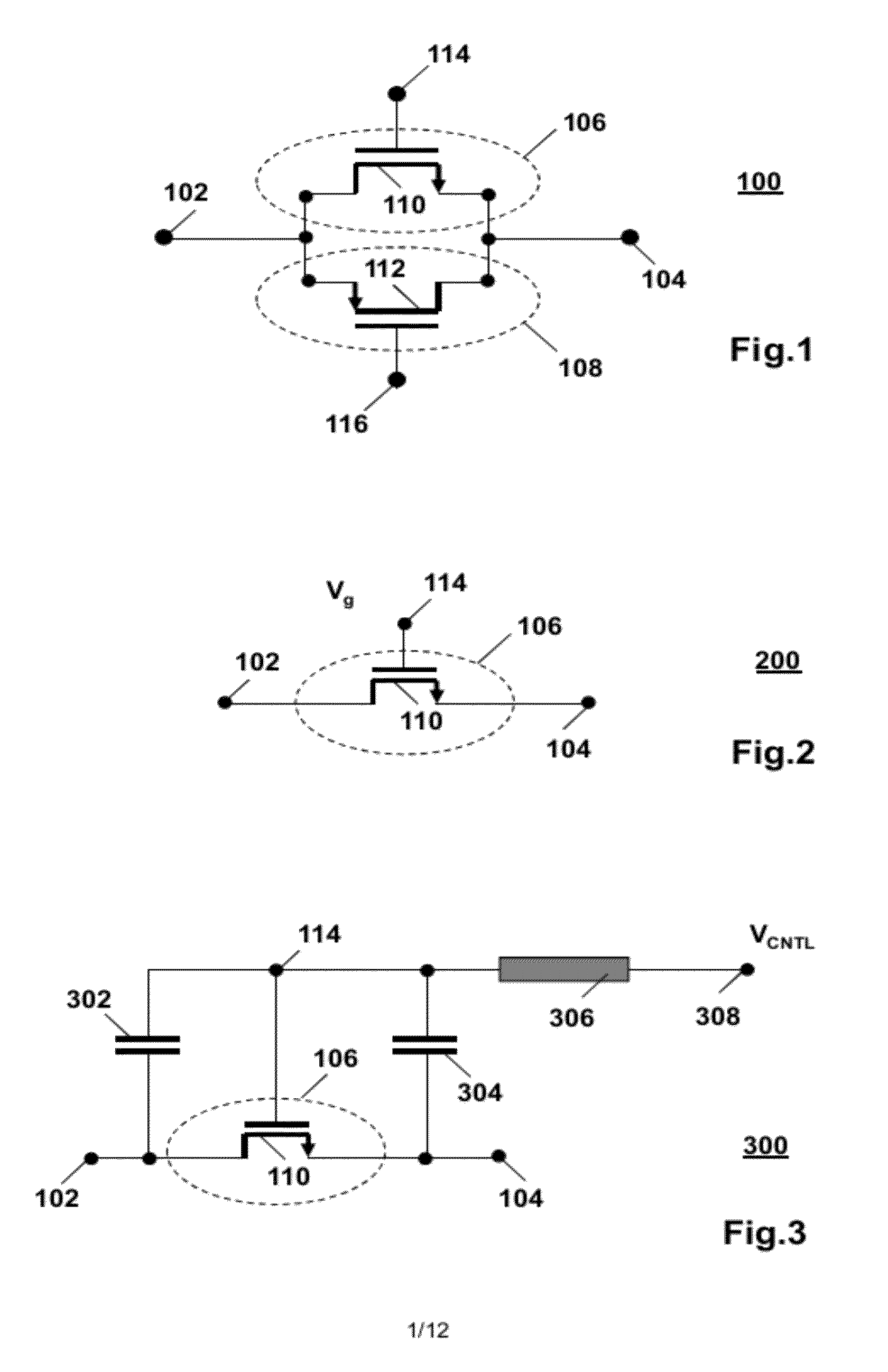
[0191]FIG. 1 is a diagram of a first conventional pass-gate 100 for controlling the passage of a signal at a first input node 102 to a first output node 104 under control of a control-voltage. The first conventional pass-gate 100 comprises a first field effect transistor (FET) 106 and a second FET 108. The first FET 106 is of an N-channel conductivity type, e.g., an NMOS FET, and the second FET 108 is of a P-channel conductivity type, e.g., a PMOS FET. The first FET 106 has a first current channel 110, and the second FET has a second current channel 112. The first current channel 110 and the second current channel 112 are connected in parallel between the first input node 102 and the first output node 104. The first FET 106 has a first control electrode 114, and the second FET has a second control electrode 116. Typically, the first control electrode 114 and the second control electrode 116 receive logically complementary control-voltages to render the first current channel 110 and ...


PUM


Abstract

A pass-gate has a passageway between an input node and an output node. The pass-gate selectively opens or closes the passageway for a signal at the input node under control of a voltage. The pass-gate has a field-effect transistor with a gate electrode and a current channel. The current channel is arranged between the input node and the output node. The gate electrode receives the voltage. The pass-gate is configured so as to have the voltage at the control electrode substantially follow the signal at the input node when the passageway is open to the signal.

Description

FIELD OF THE INVENTION[0001]The invention relates to a first electronic circuit comprising a first pass-gate with a first voltage-controlled switch for controllably passing a single-ended signal. The invention also relates to a second electronic circuit comprising a first pass-gate with a first voltage-controlled switch and a second pass-gate with a second voltage-controlled switch for controllably passing a differential signal. The invention further relates to a third electronic circuit with an M×1 multiplexer for multiplexing a number of M single-ended input signals, to a fourth electronic circuit with an 1×M demultiplexer for demultiplexing a single single-ended input signal into a number of M single-ended output signals, to a fifth electronic circuit comprising an M×1 multiplexer for multiplexing a number of M differential input signals to a single differential output signal, to a sixth electronic circuit with a 1×M demultiplexer for demultiplexing a single differential input si...

Claims


Application Information

Patent Timeline
IPC IPC(8): H03K17/687
CPCH03K17/005H03K17/145H03K17/063H03K17/007
Inventor DEN BESTEN, GERRIT WILLEM
Owner NXP BV
Why Eureka
Try Eureka