
Frequency-variable antenna circuit, antenna device constituting it, and wireless communications apparatus comprising it

a frequency-variable antenna and antenna device technology, applied in the direction of simultaneous aerial operations, antennas, elongated active element feeds, etc., can solve the problems of insufficient bandwidth, difficult to achieve impedance matching, and not simply applicable to higher-mode resonan

Active Publication Date: 2012-06-14
HITACHI METALS LTD
View PDF6 Cites 69 Cited by
  • Summary
  • Abstract
  • Description
  • Claims
  • Application Information

AI Technical Summary

Benefits of technology

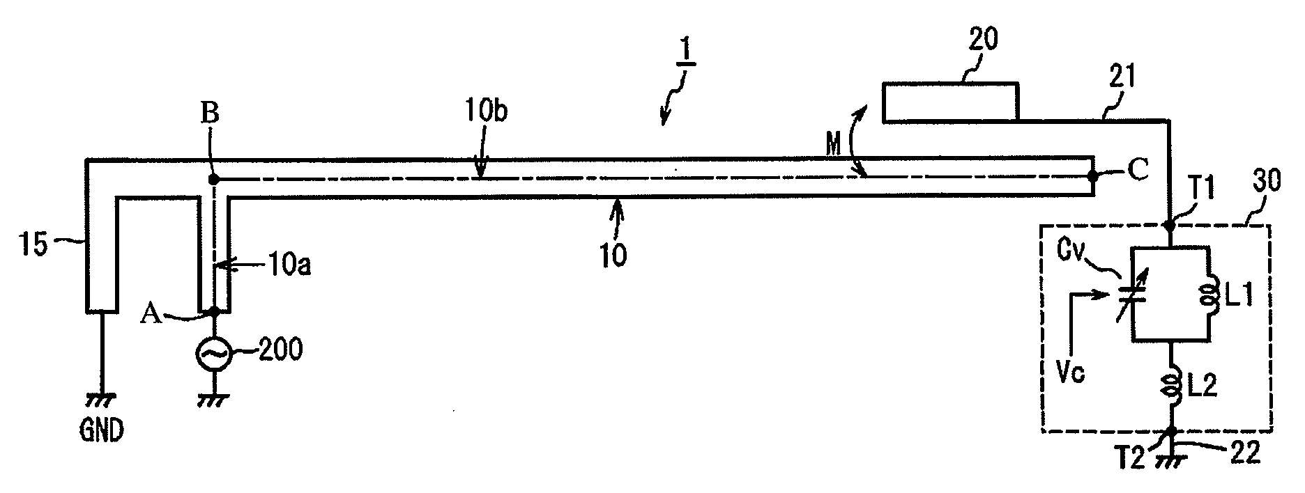
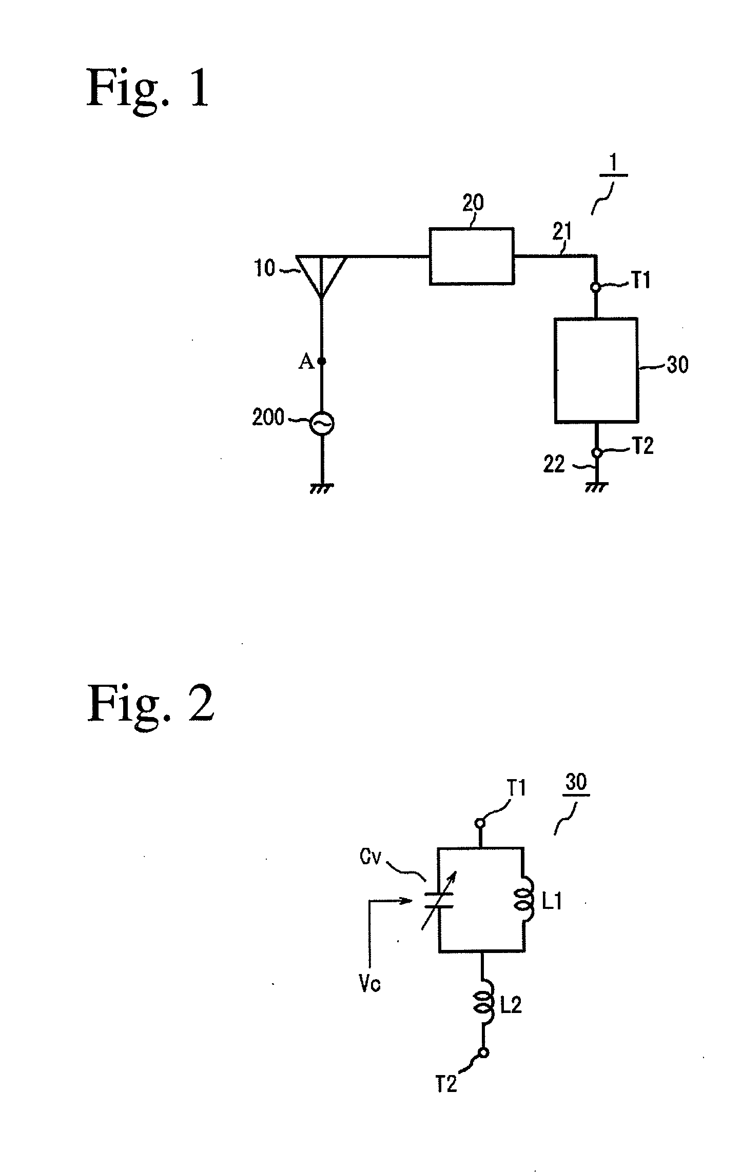
[0019]The first antenna device of the present invention for constituting a frequency-variable antenna circuit comprises a first strip-shaped antenna element and a frequency-adjusting means coupled to the first antenna element via a coupling means; the frequency-adjusting means comprising a parallel resonance circuit comprising a variable capacitance circuit and a first inductance element, and a second inductance element series-connected to the parallel resonance circuit; the first antenna element having one end acting as a feeding point and the other end acting as an open end; and part of the first antenna element being electromagnetically coupled to the coupling means.

Problems solved by technology

However, because the DCS band, the PCS band and the UMTS band have frequencies about 2-2.5 times that of the GSM (registered trademark) band, failing to meet the condition that pluralities of frequency bands have a 1:3 relation, they are not simply applicable to higher-mode resonance.
In such frequency bands, impedance matching is difficult to achieve by resonance with one antenna element, and its bandwidth is insufficient.
However, because power consumption and battery voltage have been reduced in mobile communications apparatuses such as cell phones, etc., resulting in smaller change width of voltage applied to variable capacitance diodes, the mere arrangement of a variable capacitance diode between an antenna element and a ground electrode restricts the variation range of electrostatic capacitance, so that tuning in a desired range is likely difficult.
Also, the change of electrostatic capacitance is not inversely proportional to voltage applied, making the adjustment of resonance frequency also difficult.
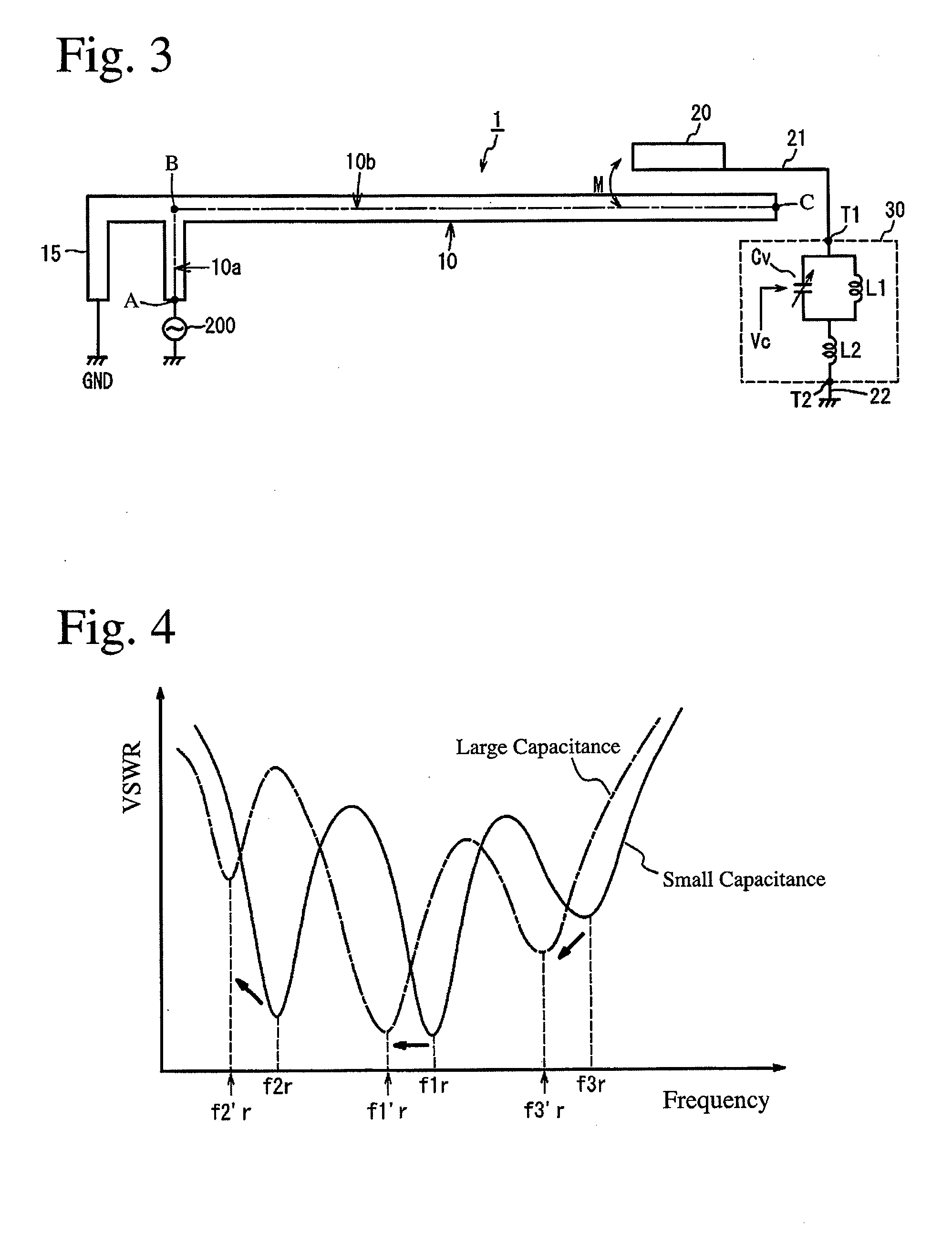
However, this antenna comprising an antenna element electromagnetically coupled to a parasitic antenna element suffers the problem that its VSWR characteristics are likely to deteriorate because the change of the resonance frequency of a low-frequency band leads to the change of the resonance frequency of a higher frequency band.
Also, because the antenna element and the parasitic antenna element are arranged on the same plane, the antenna is disadvantageously large.

Method used


Image

  • Frequency-variable antenna circuit, antenna device constituting it, and wireless communications apparatus comprising it
  • Frequency-variable antenna circuit, antenna device constituting it, and wireless communications apparatus comprising it
  • Frequency-variable antenna circuit, antenna device constituting it, and wireless communications apparatus comprising it

Examples


example 1

[0119]FIG. 26 shows one example of the frequency-variable antenna devices of the present invention capable of handling a low-frequency band and a high-frequency band, and FIGS. 27 and 28 show its appearance. In the figures, a power supply path to a variable capacitance circuit Cv in a frequency-adjusting means 30 is omitted.

[0120]The frequency-variable antenna circuit 1 is formed on an antenna board 80 separate from a main circuit board (not shown) on which a feeding circuit 200 is formed, and the antenna board 80 is connected to the main circuit board by a coaxial cable. Other connection methods include, for example, connection by pushing a grounded plate spring terminal on the main circuit board to the antenna board (called “C-clip”). In this case, a connecting portion of the antenna board comprises only a connecting electrode terminal

[0121]The antenna element 10 formed by a thin conductor plate made of Cu comprises a first antenna element 10 (comprising regions 10a, 10b, 10c and ...

example 2

[0130]FIG. 30 shows the structure of the frequency-variable antenna circuit of Example 2, and FIGS. 31 and 32 shows its appearance. Explanation will be omitted on portions of this frequency-variable antenna circuit common to those in Example 1.

[0131]The structure of the antenna element is substantially the same as in Example 1 except that a region 10f is added as the first antenna element. Because the antenna element cannot be sufficiently long in a limited space in a casing of a cell phone, a resonance frequency of a fundamental mode is finely adjusted by the region 10f to expand the resonance frequency to a desired frequency. Because larger distance from a ground electrode is preferable to improve a radiation gain, a region 10a was set as high as about 4.5 mm from a main surface of the antenna board 80.

[0132]A wide surface of the region 10b of the first antenna element 10 extends in parallel with the main surface of the antenna board 80 toward the open end F, and the first antenna...

example 3

[0138]FIG. 33 shows one example of antenna devices comprising a coupling means 20 disposed at a different position. Because the coupling means 20 is electromagnetically coupled to a region 10e of a first antenna element 10, a frequency-adjusting means 30 is separate from a feeding point A. Another dielectric chip 115 is disposed such that a region 10b of a first antenna element 10 is brought into contact with a region 12b of a second antenna element 12. Because the structures, etc. of the antenna element and the frequency-adjusting means 30 are the same as in Example 2, their explanation will be omitted.

[0139]FIG. 34 shows the dependence of average gain on a resonance frequency when the connecting path of a switch SW in a variable capacitance circuit Cv constituting the frequency-adjusting means 30 was changed in Examples 2 and 3. In both antenna devices of Examples, when the connection of the switch SW shown in FIG. 10 was changed from between ports P1 and P2 (C1 was connected) to ...


PUM


Abstract

An antenna device comprising an antenna element disposed on a mounting board separate from a main circuit board, a coupling means disposed on the mounting board such that it is electromagnetically coupled to the antenna element, and a frequency-adjusting means disposed on the mounting board such that it is connected to the coupling means, the antenna element comprising first and second strip-shaped antenna elements integrally connected for sharing a feeding point, the second antenna element being shorter than the first antenna element; the coupling means being formed on a dielectric chip attached to the mounting board, and having a coupling electrode electromagnetically coupled to part of the first antenna element. The frequency-adjusting means comprises a parallel resonance circuit comprising a variable capacitance circuit and a first inductance element, and a second inductance element series-connected to the parallel resonance circuit.

Description

FIELD OF THE INVENTION[0001]The present invention relates to a frequency-variable antenna circuit capable of changing a resonance frequency, an antenna device constituting at least part thereof, and a wireless communications apparatus comprising such antenna device for handling pluralities of frequency bands.BACKGROUND OF THE INVENTION[0002]Because of the rapid expansion of the use of wireless communications apparatuses such as cell phones, etc., more frequency band ranges have become used for communications systems. Particularly, increasing numbers of cell phones handling pluralities of transmitting / receiving bands, such as dual-band, triple-band and quad-band cell phones, have recently got used. For example, quad-band cell phones for communications systems in a GSM (registered trademark) 850 / 900 band, a DCS band, a PCS band and a UMTS band need antennas (multi-band antennas) capable of handling these frequency bands, because the GSM (registered trademark) 850 / 900 band uses a frequ...

Claims


Application Information

Patent Timeline
IPC IPC(8): H01Q9/36H01Q5/10H01Q5/15
CPCH01Q5/392H01Q9/42
Inventor HAYASHI, KENJIOKAMOTO, HIROSHIIDENO, HIROTO
Owner HITACHI METALS LTD
Learn More