Liquid crystal display device

Active Publication Date: 2018-03-08
TOPPAN PRINTING CO LTD
View PDF6 Cites 10 Cited by
  • Summary
  • Abstract
  • Description
  • Claims
  • Application Information

AI Technical Summary

Problems solved by technology

However, in the in-cell structure, a problem arises in the touch sensing technique which is not mentioned in the above-mentioned patent literature.
In other words, there is a problem which is unlikely to arise in an external touch panel structure, that is, a new technical problem that noise is induced from the source wiring electrically coupled to the active elements provided in the liquid crystal cells.
The techniques disclosed in PTLs 1 to 6 fail to suggest means for reducing noise coming from the source wiring to which i

Method used


Image

  • Liquid crystal display device
  • Liquid crystal display device
  • Liquid crystal display device

Examples


first embodiment

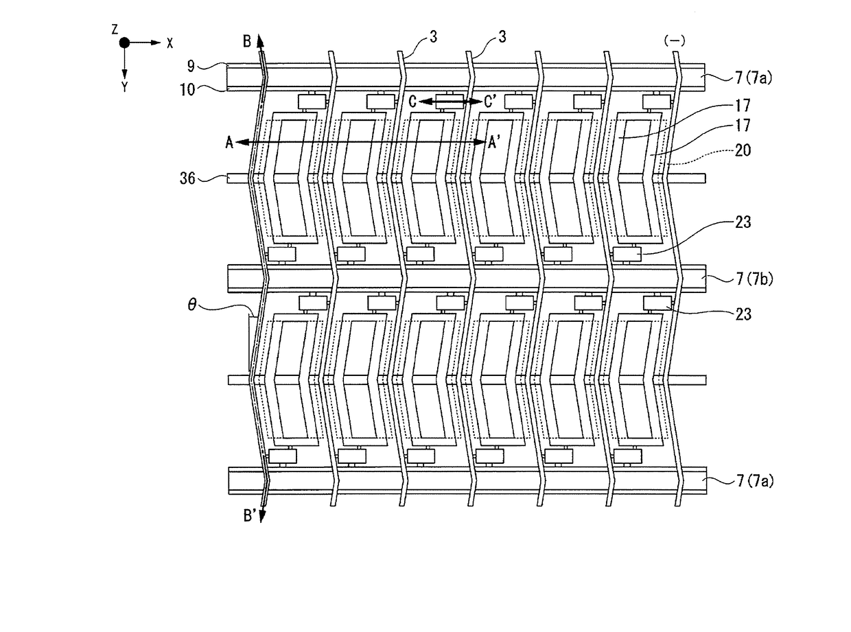
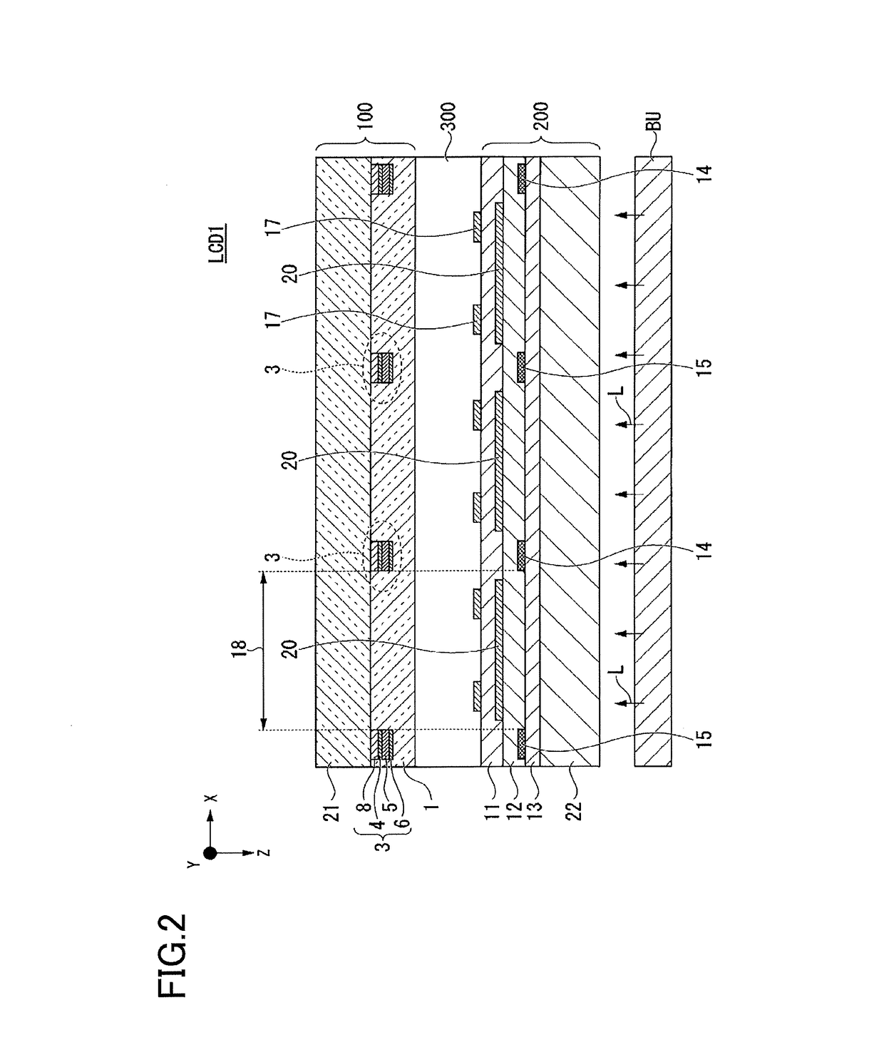
[0063](Configuration of Liquid Crystal Display Device LCD1)

[0064]Hereinafter, with reference to FIGS. 1 to 15, a first embodiment of the liquid crystal display device of the present invention will be described.

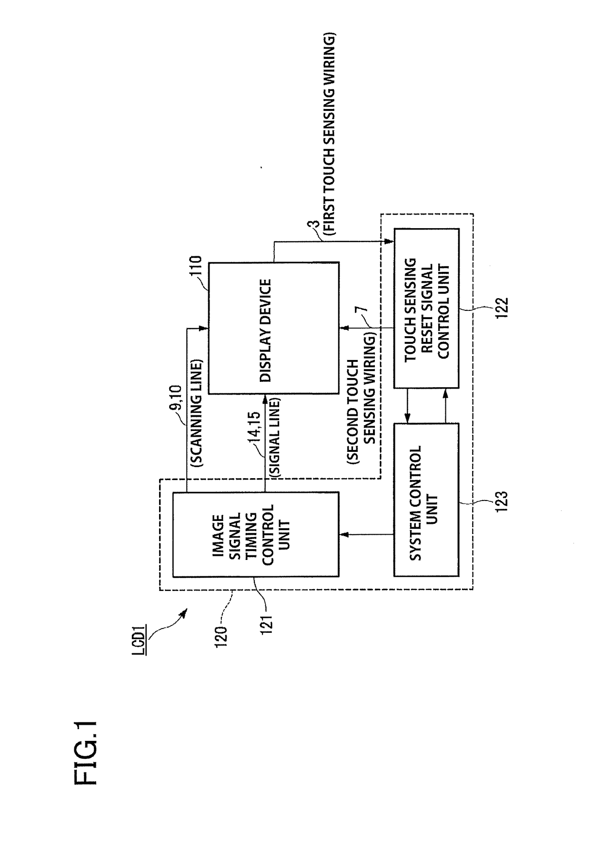
[0065]FIG. 1 is a block diagram showing a liquid crystal display device according to the first embodiment of the present invention. As shown in FIG. 1, a liquid crystal display device LCD1 is provided with a display device 110 and a control unit 120 that controls the display device 110 and a touch sensing function. The control unit 120 has a publicly known configuration, including an image signal timing control unit 121 (first control unit), a touch sensing reset signal control unit 122 (second control unit) and a system control unit 123 (third control unit).

[0066]The image signal timing control unit 121 sets the common electrode 20 (described later) provided on the array substrate 200 to a constant potential, and transmits signals to the gate wirings 9 and 10 (scanning line w...

second embodiment

[0205]The liquid crystal display device according to the second embodiment will be described with reference to FIGS. 1, 12 and 16 to 28.

[0206]According to a liquid crystal display device LCD2, a transparent electrode is provided on the display device substrate 100, liquid crystal molecules having negative dielectric anisotropy constitute the liquid crystal layer 300, and the common electrode 20 is not provided on the array substrate 200. Hence, a vertical electric field method is used for the liquid crystal display device LCD2. In the method, vertical electric field is applied to the liquid crystal layer 300 sandwiched between the transparent electrode and the pixel electrode, thereby driving the liquid crystal layer 300. Further, the liquid crystal driving is controlled by the first active element 28a and the second active element 28b which are connected to the pixel electrode 17.

[0207]In the liquid crystal display device LCD2, the image signal timing control unit 121 shown in FIG....

third embodiment

Modification of Third Embodiment

[0298]Next, modification of the liquid crystal display device according to the third embodiment of the present invention will be described with reference to FIGS. 29, 30, 34 and 35. FIG. 34 is a cross-sectional view sectioned across the E-E′ line of FIG. 29. FIG. 35 is a cross-sectional view sectioned across the F-F′ line of FIG. 29, partly showing a modification of the liquid crystal display device according to the third embodiment of the present invention, and illustrating an electrostatic capacitance C3 produced between the first touch sensing wiring 3 serving as the touch detection wiring and the second touch sensing wiring 7 serving as the touch drive wiring.

[0299]The modification of the third embodiment differs from the third embodiment in the locations of the black matrix BM with respect to the color filter.

[0300]As shown in FIG. 34, the first touch sensing wiring 3 is provided on the black matrix BM, and at a location corresponding to the ITO ...


PUM


Abstract

A liquid crystal display device includes a display device substrate including a first touch sensing wiring, an array substrate including a second touch sensing wiring orthogonally intersecting the first touch sensing wiring, a liquid crystal layer disposed between the display device substrate and the array substrate, a controller that supplies a positive first image signal to the first source wiring, supplies a negative second image to the second source wiring, applies a liquid crystal display voltage between the pixel electrode and the common electrode being synchronized to supply of the first image signal and the second image signal, thereby driving the liquid crystal layer, performing an image display, and applying a voltage to the second touch sensing wiring after performing the image display.

Description

CROSS-REFERENCE TO RELATED APPLICATIONS[0001]The present application is a continuation of International Application No. PCT / JP2015 / 063761, filed May 13, 2015, the entire contents of which are incorporated herein by reference.BACKGROUND OF THE INVENTIONField of the Invention[0002]The present invention relates to liquid crystal display devices capable of performing stable touch sensing operations and having high sensitivity in touch sensing. The present invention relates to liquid crystal display devices capable of operating with fast response.Discussion of the Background[0003]Liquid crystal display devices have been used for large display devices such as televisions, tablet devices, smartphones and the like. The liquid crystal display device may be configured such that a liquid crystal layer is disposed between two transparent substrates made of glass or the like. Major liquid crystal driving methods for such liquid crystal devices are roughly classified into a VA (vertical alignment...

Claims


Application Information

Patent Timeline
IPC IPC(8): G06F3/047G06F3/044G06F3/041G02F1/1343G02F1/1368
CPCG06F3/047G06F3/044G06F3/0412G02F1/1343G06F3/0416G02F1/1368G06F3/04166G06F3/0445G06F3/0446G02F1/1333G06F3/041
Inventor KIMURA, YUKIHIROFUKUYOSHI, KENZO
Owner TOPPAN PRINTING CO LTD
Why Eureka
Try Eureka