Wavelength monitor

a monitor and wavelength technology, applied in the field of wavelength monitors, can solve the problems of increasing maintenance costs, increasing the size of the whole wavelength-variable light source, and increasing costs

Inactive Publication Date: 2012-06-14
MITSUBISHI ELECTRIC CORP
View PDF4 Cites 50 Cited by
  • Summary
  • Abstract
  • Description
  • Claims
  • Application Information

AI Technical Summary

Benefits of technology

[0010]It is an object of the present invention to at least partially solve the problems in the conventional technology.

Problems solved by technology

For performing a stable management, this WDM system needs to ensure a preparatory signal light source having the same oscillation wavelength in case of unexpected stoppage of a signal light source, which increases the maintenance cost.
However, there are following problems in the above conventional technologies.
Moreover, because an optical component such as the beam splitter is needed, the size of the whole wavelength-variable light source increases and accordingly the cost increases.
In the conventional method (for example, Non-patent document 4) of performing the wavelength monitoring by using exit light in the backward direction, although the above problems are solved, a point at which light is emitted from a semiconductor substrate (hereinafter may be referred to just as an “exit portion”) is different for each semiconductor laser, so that a variation in the wavelength monitoring characteristics due to an angle of incident on a filter and an incident position on the filter is a problem.
The frequency periodicity of the transmittance of the filter depends on the incident angle of light, so that the relationship between the light intensity of exit light from each semiconductor laser detected by a photodetector and the frequency of light becomes different, which degrades the monitoring accuracy of the wavelength of light.

Method used


Image

  • Wavelength monitor
  • Wavelength monitor
  • Wavelength monitor

Examples


first embodiment

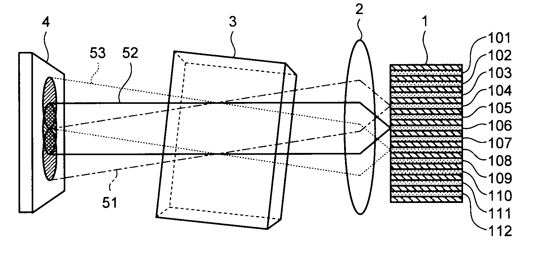
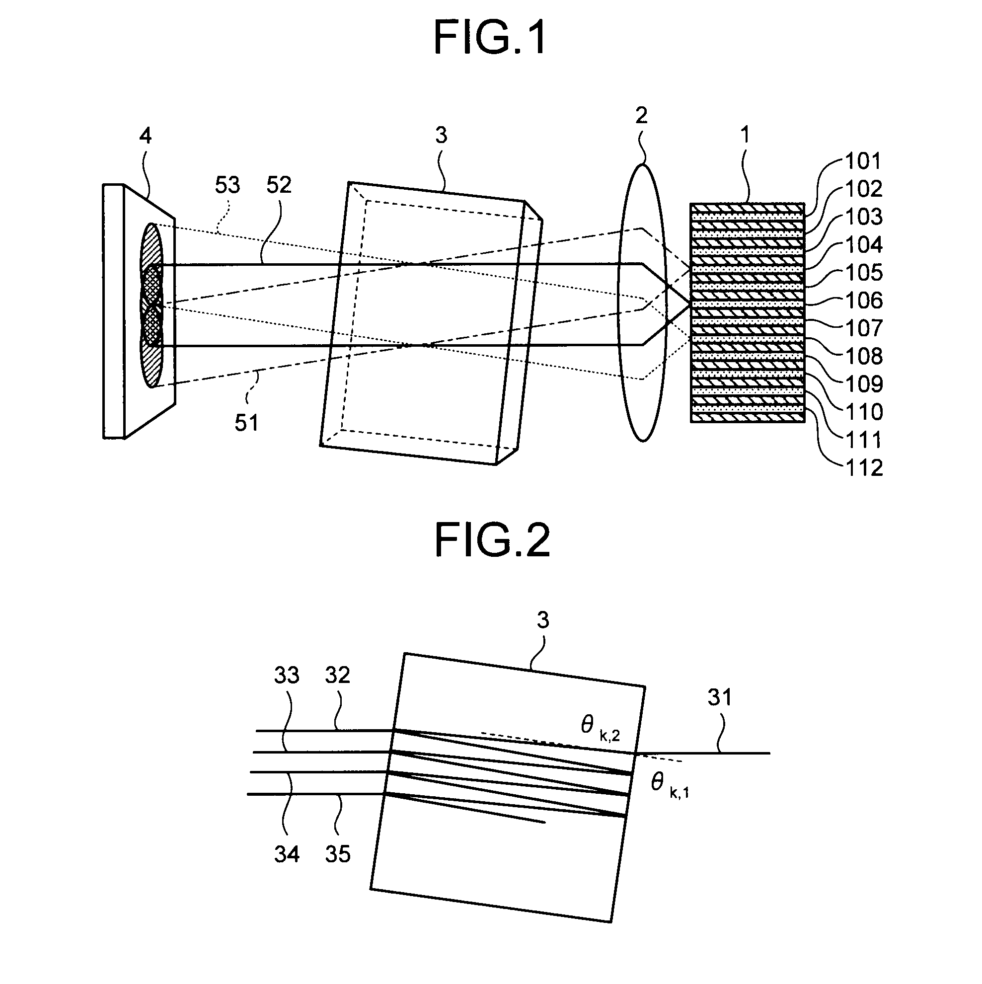
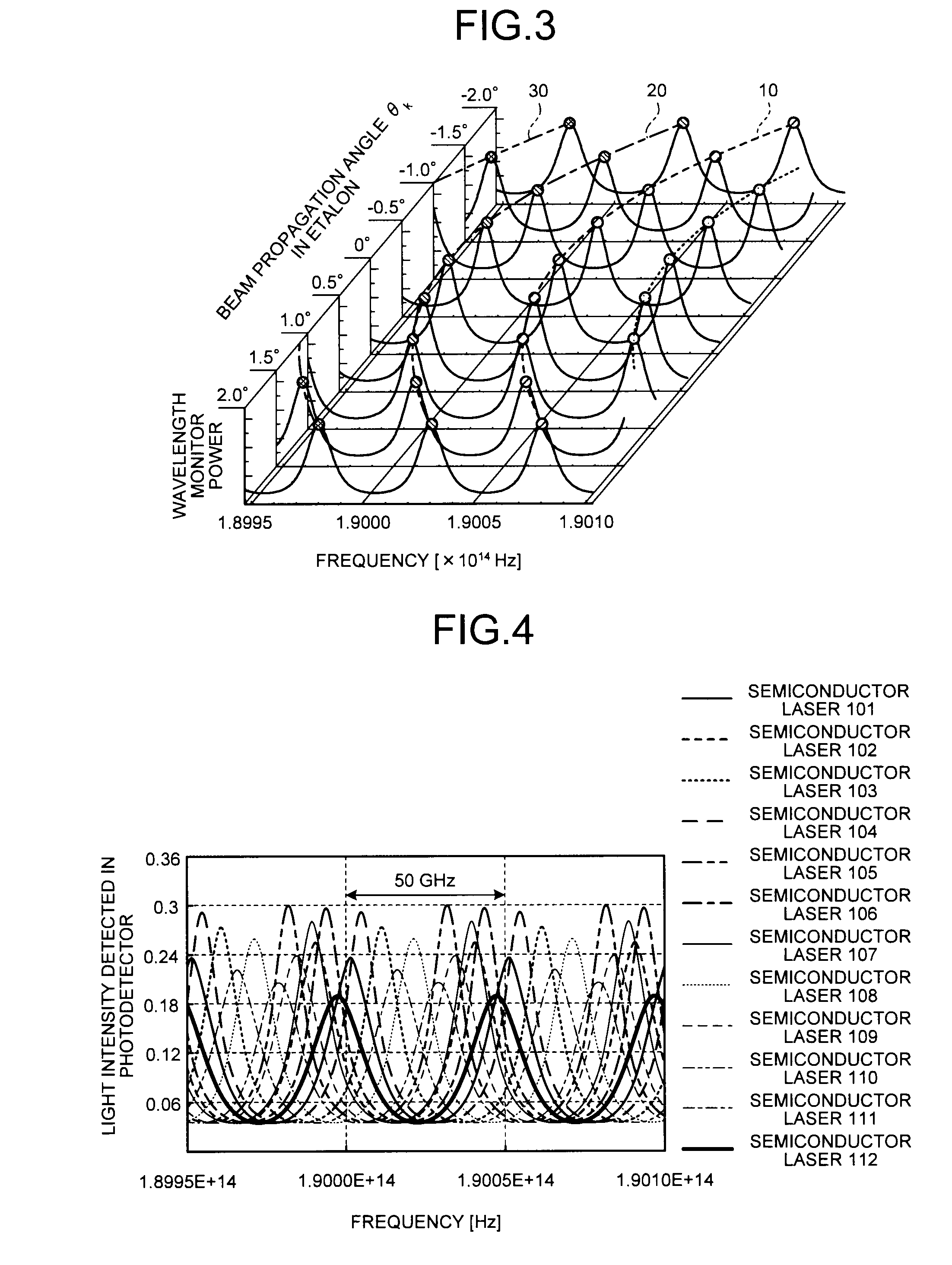
[0023]FIG. 1 is a diagram illustrating a configuration of a wavelength monitor according to the first embodiment of the present invention. The wavelength monitor according to the present embodiment is provided in a wavelength-variable optical module (not shown) capable of changing the wavelength of exit light, and includes a semiconductor substrate 1, two or more semiconductor lasers 101 to 112 formed in parallel on the semiconductor substrate 1, a collimating lens 2 that collimates diffusion light emitted from the semiconductor lasers 101 to 112 into parallel light, a filter (for example, an etalon 3) that is arranged in the backward of the semiconductor substrate 1 so that collimated light transmitted through the collimating lens 2 enters and has a periodic frequency dependence of the transmittance, and a photodetector 4 that receives light transmitted through the etalon 3 and detects the light intensity thereof.

[0024]In FIG. 1, as one example, a beam path 51 of a beam emitted fro...

second embodiment

[0047]FIG. 6 is a diagram illustrating a configuration of a wavelength monitor according to the second embodiment of the present invention. The wavelength monitor shown in FIG. 6 includes the semiconductor substrate 1, two or more semiconductor lasers 101 to 112 formed in parallel on the semiconductor substrate 1, optical waveguides 121 to 132 that function to confine light in a small area and guide the light in a specific direction, the collimating lens 2 that collimates diffused light emitted from the optical waveguides 121 to 132 into parallel light, a filter, for example, the etalon 3, which is arranged in the backward direction of the semiconductor substrate 1 so that the collimated light transmitted through the collimating lens 2 enters and has a periodic frequency dependence of the transmittance, and the photodetector 4 that receives the light transmitted through the etalon 3 and detects the light intensity. The optical waveguides 121 to 132 are arranged such that the positio...

third embodiment

[0051]FIG. 7 is a diagram illustrating a configuration of a wavelength monitor according to the third embodiment of the present invention. The present embodiment is a modified example of the first and second embodiments, wherein the wavelength monitor includes the semiconductor substrate 1, two or more semiconductor lasers 101 to 112 formed in parallel on the semiconductor substrate 1, the optical waveguides 121 to 132 (not shown, as can be optional and have the same structure as those shown in FIG. 6) that function to confine light beam in a small area and guide the light in a specific direction, the collimating lens 2 that collimates diffused light emitted from the optical waveguides 121 to 132 into parallel light, a filter, for example, the etalon 3, which is arranged in the backward direction of the semiconductor substrate 1 so that the collimated light transmitted through the collimating lens 2 enters and has a periodic frequency dependence of the transmittance, the photodetect...


PUM


Abstract

In a wavelength monitor that monitors a wavelength of laser light emitted from at least two semiconductor lasers formed in parallel on a semiconductor substrate, the wavelength monitor includes a collimating lens that collimates laser light from each of the semiconductor lasers, an etalon that is arranged so that laser light collimated by the collimating lens is capable of entering and has a periodicity, and a photodetector that receives laser light transmitted through the etalon and detects a light intensity, wherein a beam propagation angle in the etalon of laser light emitted from each of the semiconductor lasers becomes a predetermined angle obtained by formula 1.

Description

BACKGROUND OF THE INVENTION[0001]1. Field of the Invention[0002]The present invention relates to a wavelength monitor.[0003]2. Description of the Related Art[0004]Recently, in the field of optical communications, with the increase in speed and capacity in an optical transmission system, the Wavelength Division Multiplexing (WDM) system for performing optical multiple transmission with one optical fiber has become widespread as a core technology thereof. For performing a stable management, this WDM system needs to ensure a preparatory signal light source having the same oscillation wavelength in case of unexpected stoppage of a signal light source, which increases the maintenance cost. For suppressing this cost, a demand for an optical wavelength-variable light source capable of outputting laser light of a plurality of wavelengths by one signal light source has been increasing.[0005]It is required for the wavelength-variable light source that the wavelength of an optical signal is st...

Claims


Application Information

Patent Timeline
Patent Type & Authority Applications(United States)
IPC IPC(8): G01J1/42
CPCH01S5/0014H01S5/4025H01S5/0687H01S5/0071
Inventor MOCHIZUKI, KEITAARUGA, HIROSHISUGITATSU, ATSUSHI
Owner MITSUBISHI ELECTRIC CORP
Why Eureka
Try Eureka