
Visual Inspection Method And Apparatus And Image Analysis System

a technology of visual inspection and image analysis, applied in the field of visual inspection, can solve the problems of difficult suitable region setting and long time-consuming review

Inactive Publication Date: 2012-06-21
HITACHI HIGH-TECH CORP
View PDF2 Cites 13 Cited by
  • Summary
  • Abstract
  • Description
  • Claims
  • Application Information

AI Technical Summary

Benefits of technology

The method achieves high sensitivity in defect detection while suppressing false alarms, simplifying the process of setting false alarm judgment criteria and improving inspection efficiency by automatically selecting features and setting thresholds.

Problems solved by technology

Accordingly, there is a problem of requiring a long time in reviewing.
Although it is also possible to perform the defect judgment using a threshold which is different for every region obtained after division without reviewing, in that case, there is a problem that a suitable region setting is difficult since it is necessary to decide the region, without a proper guideline.

Method used


Image

  • Visual Inspection Method And Apparatus And Image Analysis System
  • Visual Inspection Method And Apparatus And Image Analysis System
  • Visual Inspection Method And Apparatus And Image Analysis System

Examples


embodiment 1

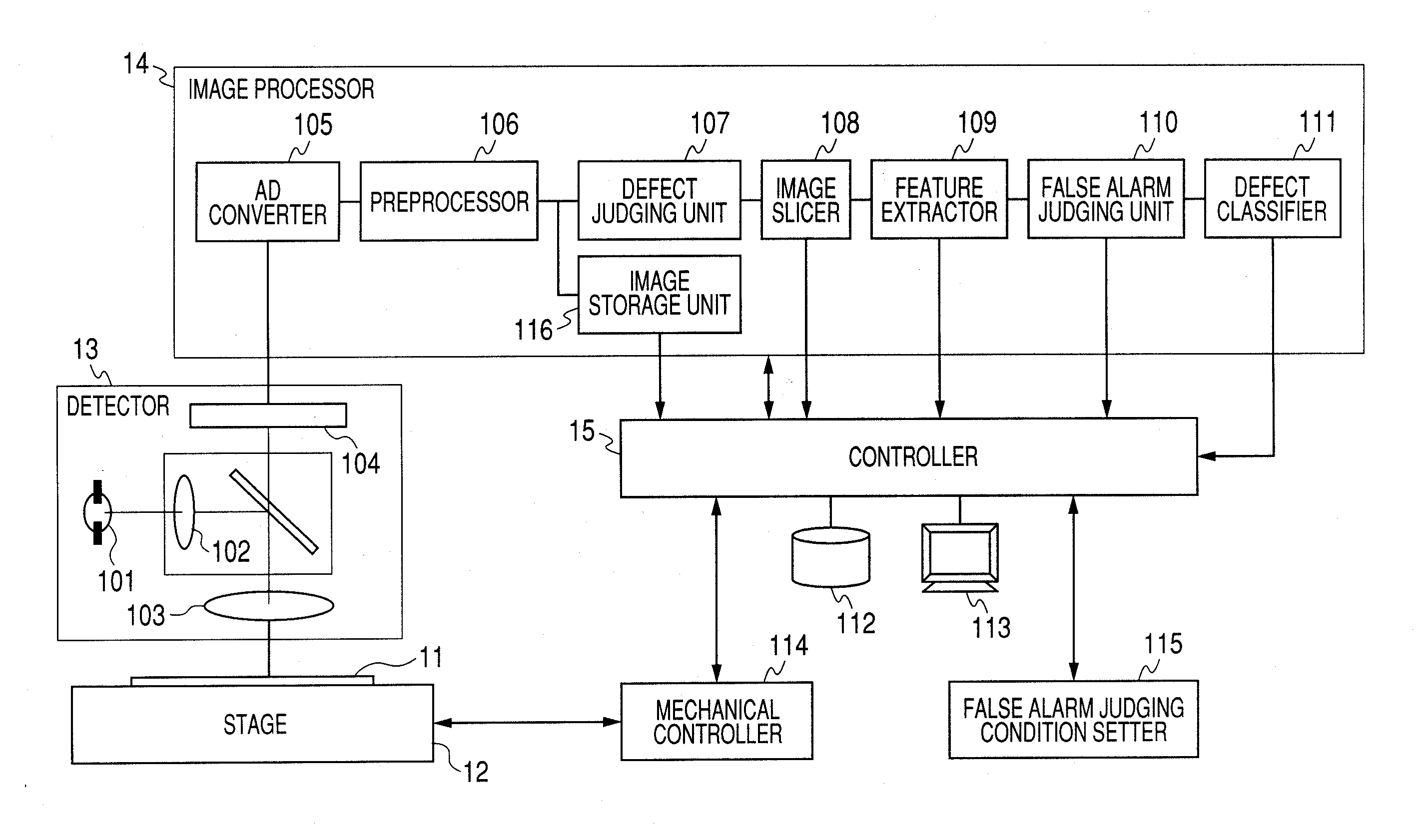
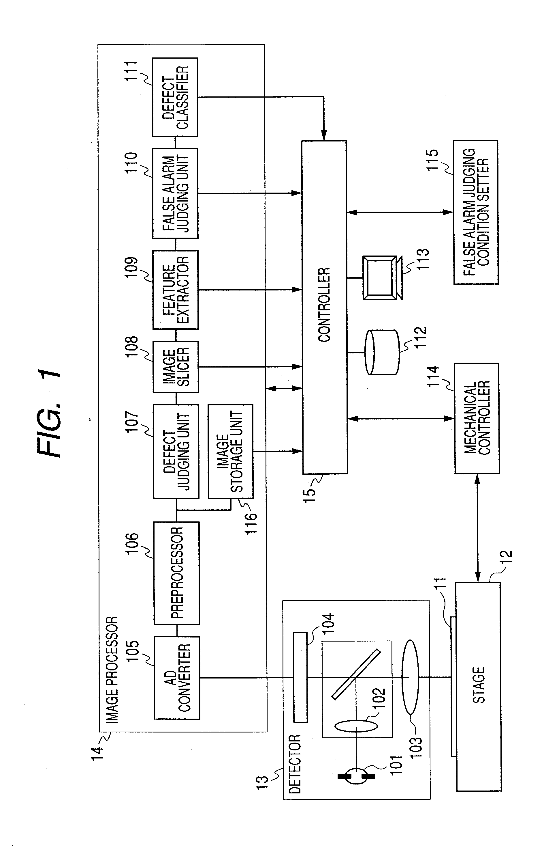
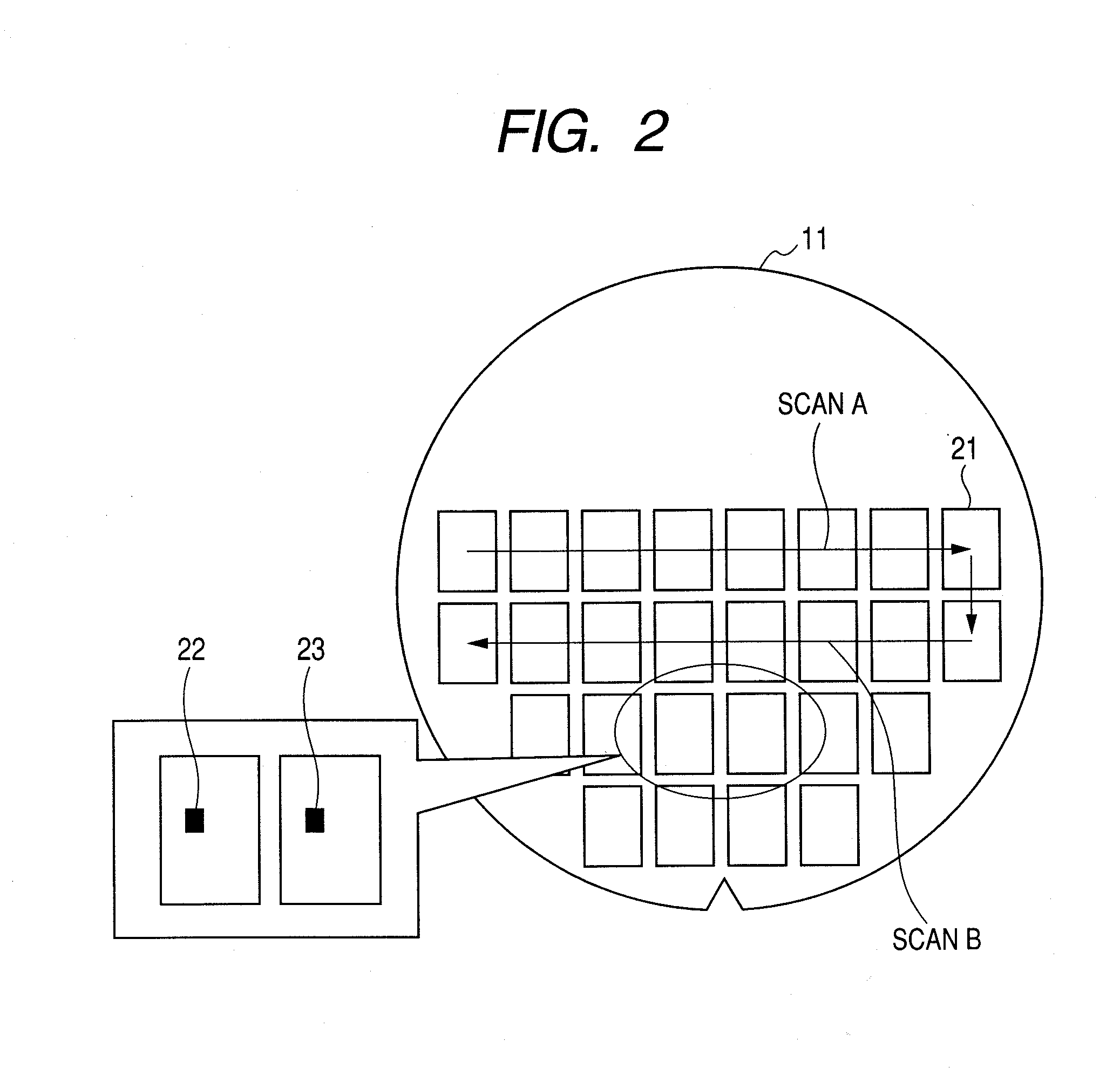
[0035]A first embodiment of the present invention is described in detail with reference to FIGS. 1 to 16. The present embodiment takes for an example an optical visual inspection apparatus for a semiconductor wafer. FIG. 1 illustrates an exemplified structure of the optical visual inspection apparatus. The optical visual inspection apparatus according to the present embodiment includes a stage 12 which mounts and moves an inspecting object 11 such as a semiconductor wafer, a detector 13, a light source 101 for illuminating the inspecting object 11, an illumination optical system 102 which condenses the light emitted from the light source 101, an objective lens 103 which illuminates the inspecting object 11 by the illumination light condensed by the illumination optical system 102 and provides an image by forming the reflected optical image, an image sensor 104 which converts into a image signal the formed optical image corresponding to the brightness thereof. An image processor 14 d...

embodiment 2

[0083]In Embodiment 1, the false alarm judging condition setter 115 is included in the inspection apparatus; however, the false alarm judging condition setter 115 may be separated from the inspection apparatus, and may be included in an off-line image analysis system. The following explains an image analysis system according to a second embodiment of the present invention with reference to FIGS. 18 and 19. FIG. 18 shows an example of structure of the image analysis system according to the second embodiment of the present invention. The image analysis system provides simplification of the defect judgment, the false alarm judgment, and the conditioning of the defect classification which are processed in the image processor 14 of the inspection apparatus.

[0084]As illustrated in FIG. 18, the image analysis system includes a defect judging simulator 1801, a defect re-judging simulator 1802, a false alarm judging simulator 1803, and a defect classification simulator 1804. When using the i...

embodiment 3

[0101]Embodiment 2 enables the conditioning of the defect judgment, false alarm judgment, and defect classification of the inspection apparatus using the information on one wafer as mentioned above. In contrast, the present embodiment performs such conditioning using the information on plural wafers. The following explains about an image analysis system according to a third embodiment of the present invention, with reference to FIG. 20. FIG. 20 is an exemplified diagram illustrating structure of the image analysis system according to the third embodiment of the present invention.

[0102]An inspection apparatus 10 inspects a wafer and outputs an inspection result. The inspection result includes information on coordinates of a detected defect, a feature, a defect class by the inspection apparatus, an inspection image, etc., with additional information to specify a wafer, such as a wafer number, a lot number, a product class, and process, and other additional information to specify inspe...


PUM


Abstract

A visual inspection method and apparatus detecting a defect with the use of a detected signal obtained by illuminating one of a light and an electron beam onto a substrate to be inspected. The visual inspection method and apparatus includes calculation of an image feature based on an image of the detected defect, calculation of a coordinate feature based on position information of the detected defect, and outputting of real defect information by performing false alarm judgment by processing with respect to one of the image feature and the coordinate feature.

Description

CROSS REFERENCE TO RELATED APPLICATION[0001]This application is a continuation of U.S. application Ser. No. 12 / 141,947, filed Jun. 19, 2008, the contents of which are incorporated herein by reference.CLAIM OF PRIORITY[0002]The present application claims priority from Japanese Patent Application JP 2007-162770 filed on Jun. 20, 2007, the content of which is hereby incorporated by reference into this application.BACKGROUND OF THE INVENTION[0003]The present invention relates to a visual inspection method and apparatus which perform detection and classification of defect, such as a fine pattern defect and a foreign particle, based on an image of an object obtained using a light of a lamp, a light of a laser, or an electron beam, for thin film devices such as a semiconductor wafer, TFT, and a photomask. The present invention relates especially to a visual inspection method and apparatus which are suitable to conduct the visual inspection of a semiconductor wafer.[0004]Thin film devices, ...

Claims


Application Information

Patent Timeline
Patent Type & Authority Applications(United States)
IPC IPC(8): G06K9/46
CPCG06T2207/30148G06T7/0004
Inventor SHIBUYA, HISAEMAEDA, SHUNJI
Owner HITACHI HIGH-TECH CORP
Learn More