Sensor chip, detection device, and method of manufacturing sensor chip

a sensor chip and detection device technology, applied in the direction of optical radiation measurement, instruments, spectrometry/spectrophotometry/monochromators, etc., can solve the problems of large number of fine metal particles wasted, low variation of detecting the variation in the vicinity of the fine metal particle, and limited improvement of sensor sensitivity, etc., to achieve high sensitivity

Inactive Publication Date: 2012-06-28
SEIKO EPSON CORP
View PDF9 Cites 21 Cited by
  • Summary
  • Abstract
  • Description
  • Claims
  • Application Information

AI Technical Summary

Benefits of technology

[0026]According to this application example of the invention, the fine metal particles having the size in the order of several nanometers are arranged on the sensor chip so as to be aligned with minute gaps, and it results that the localized surface plasmon resonan

Problems solved by technology

Therefore, the signal variation for detecting the variation in the medium in the vicinity of the fine metal particle is low, and the improvement in the sensor sensitivity is limited.
In such a method there is a

Method used


Image

  • Sensor chip, detection device, and method of manufacturing sensor chip
  • Sensor chip, detection device, and method of manufacturing sensor chip
  • Sensor chip, detection device, and method of manufacturing sensor chip

Examples


first embodiment

Sensor Chip / First Embodiment

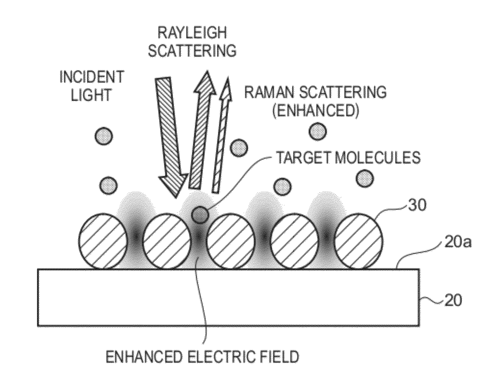
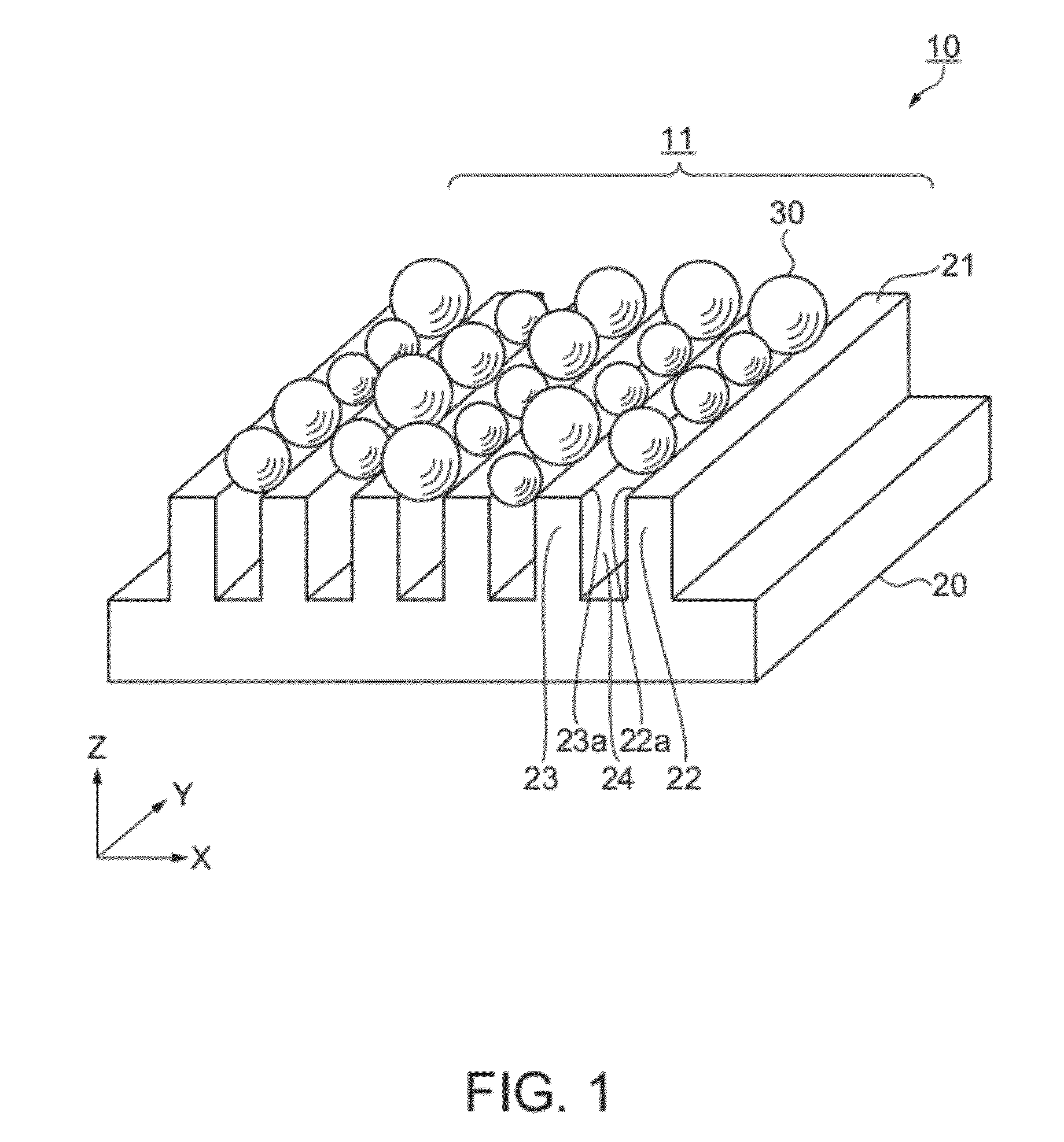
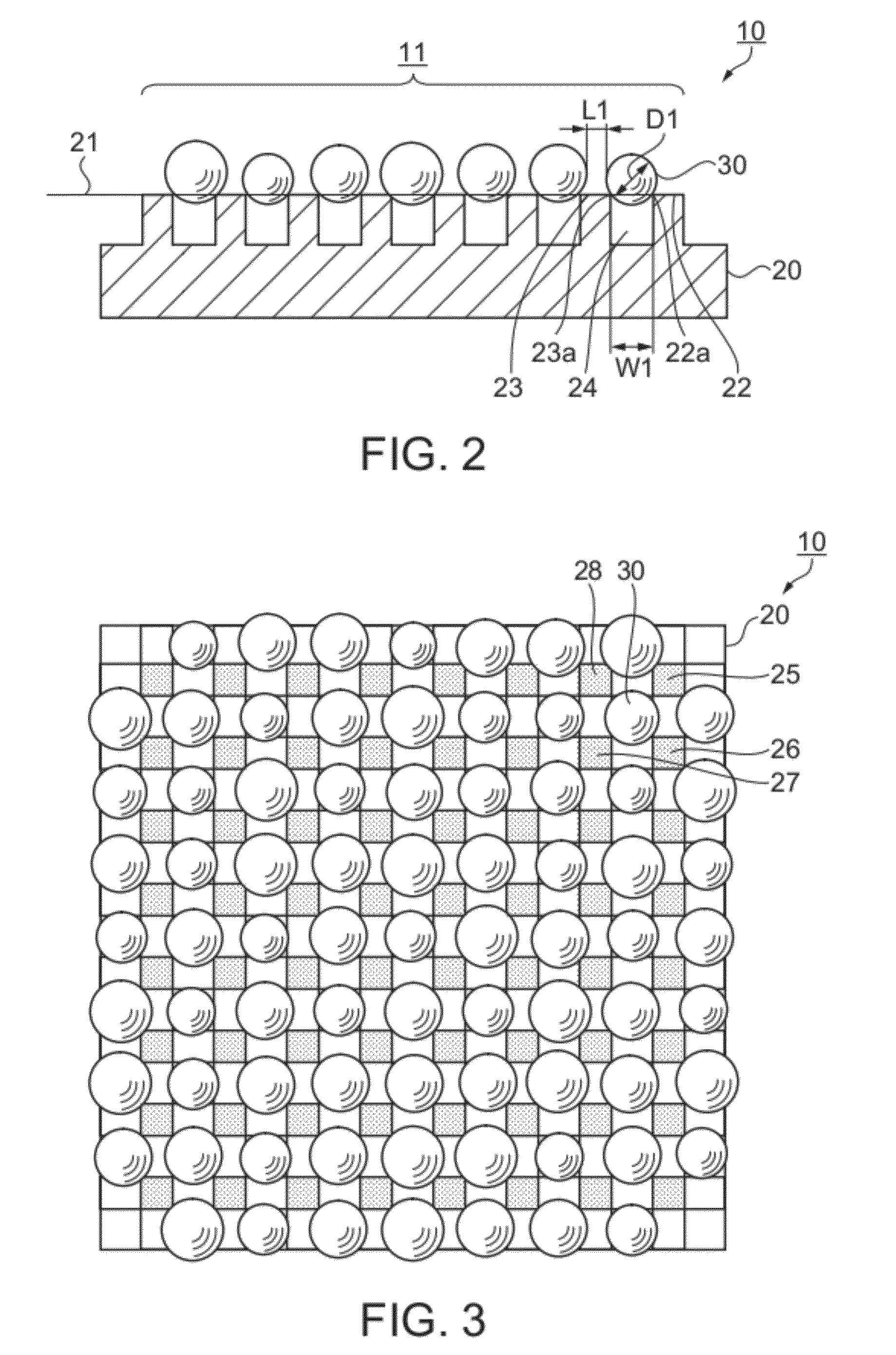
[0045]FIG. 1 is a perspective view showing a part of a sensor chip according to a first embodiment of the invention, and FIG. 2 is a cross-sectional view of the sensor chip. In FIGS. 1 and 2, the sensor chip 10 is composed of a relief structure formed on a surface of a substrate 20, and an aggregate of a number of fine metal particles 30. The area composed of the relief structure and the fine metal particles is defined as a sensor section 11. The material of the substrate 20 is made of a dielectric substance, and quartz, quartz crystal, glass such as borosilicate glass, silicon, and so on are suitable therefor. In the case of setting the incident light to the substrate 20 side, the substrate which is transparent with respect to the incident light is suitable, and in the case of setting the incident light to the fine metal particle side, the transparent substrate is not necessarily required.

[0046]The relief structure is formed to have a linear grating shap...

second embodiment

Sensor Chip / Second Embodiment

[0050]Subsequently, a sensor chip according to a second embodiment of the invention will be explained with reference to the accompanying drawings. The second embodiment is characterized in that the relief structure is formed to have a grid shape having a two-dimensional structure.

[0051]FIG. 3 is a plan view showing a part of the sensor chip according to the second embodiment. It should be noted that the cross-sectional structure can be expressed similarly to FIG. 2, and is therefore omitted. In FIG. 3, the relief structure has the protruding sections and the recessed sections arranged in each of the vertical and horizontal directions. Here, in the explanation showing one of the fine metal particles as an example, the fine metal particles 30 is arranged to be supported by four apexes at which respective ridgelines of the columnar protruding sections 25, 26, 27, and 28 intersect each other. In other words, setting a combination of the four intersections of...

third embodiment

Sensor Chip / Third Embodiment

[0064]Subsequently, a sensor chip according to a third embodiment of the invention will be explained with reference to the accompanying drawings. The third embodiment is characterized by being different from the first and second embodiments in the cross-sectional shape of the relief structure. Therefore, the different point will be explained.

[0065]FIG. 7 is a cross-sectional view showing a part of the sensor chip according to the third embodiment. In FIG. 7, the recessed sections of the relief structure are each formed having tilted walls (a tapered shape) with the bottom width narrower than the width on the upper surface 21 of the substrate 20. Such a shape can be applied to both of the one-dimensional structure of the first embodiment and the two-dimensional structure of the second embodiment described above (the case of the first embodiment is shown in the drawing). The fine metal particles 30 are each held by the protruding sections 22, 23 to thereby ...


PUM


Abstract

A sensor chip includes a substrate, a relief structure composed of protruding sections formed so as to be arranged on a surface of the substrate to have a lattice shape and a recessed section between the protruding sections, and fine metal particles arranged along upper ridge lines of the respective protruding sections of the relief structure, the protruding sections being adjacent to each other, having a minute gap with which the surface plasmon resonance occurs. By irradiating the gap between the fine metal particles with a laser beam, the localized surface plasmon resonance occurs more efficiently. As a result, the sensor chip capable of taking out the surface enhanced Raman scattering to thereby detect the substance with high sensitivity can be realized.

Description

BACKGROUND[0001]1. Technical Field[0002]The present invention relates to a sensor chip, a detection device using the sensor chip, and a method of manufacturing the sensor chip.[0003]2. Related Art[0004]Recent years, demand for sensors used for medical diagnostics or inspections of food and drink has increased, and further, development of a sensor and a detection device small in size and capable of performing sensing at high speed has been demanded. In order to meet such demand, a variety of types of sensors such as a sensor using an electrochemical process have been studied. Among these sensors, sensors using surface plasmon resonance (SPR) have been receiving increasing attention on the ground of possibility of integration, low cost, and applicability in all measurement environments.[0005]Due to the background described above, with a goal of improvement in sensor sensitivity, there has been proposed a sensor utilizing localized surface plasmon resonance (LSPR) using fine metal part...

Claims


Application Information

Patent Timeline
IPC IPC(8): G01J3/44B05D5/12G01N21/55G01N21/01G01N21/27G01N21/41G01N21/65
CPCG01N21/658G01N21/554H01L27/1446G01N21/27G01N21/55G01N21/65G01J3/44
Inventor SAKAGAMI, YUSUKE
Owner SEIKO EPSON CORP
Why Eureka
Try Eureka