Semiconductor light emitting device

a technology of light-emitting devices and semiconductors, which is applied in the direction of semiconductor devices, basic electric elements, electrical equipment, etc., can solve the problems of difficult cannot be expected to improve both, so as to improve the flow and diffusion of electric current, enhance the injection of holes, and improve the effect of electric current flow

Inactive Publication Date: 2012-07-05
QUANTUM DEVICES
View PDF3 Cites 4 Cited by
  • Summary
  • Abstract
  • Description
  • Claims
  • Application Information

AI Technical Summary

Benefits of technology

[0016]As described above, there is provided a semiconductor light emitting device which can improve flow of an electric current between an electrode and a semiconductor layer, uniformize diffusion thereof, and enhance injection of holes, thereby maximizing efficiency.

Problems solved by technology

However, the conventional transparent electrode 107 doped with either of the n-type impurities or the p-type impurities could improve one of the diffusion of an electric current or the injection of holes but could not be expected to improve both of them.
For example, in the case that the transparent electrode 107 is formed using ZnO on a GaN-based semiconductor layer, if the transparent electrode 107 is doped with only the p-type impurities, the injection of holes is enhanced to some extent by increasing hole concentration but it is difficult to improve the flow and diffusion of an electric current.

Method used


Image

  • Semiconductor light emitting device
  • Semiconductor light emitting device
  • Semiconductor light emitting device

Examples


Embodiment Construction

Technical Problems

[0008]Accordingly, one or more exemplary embodiments provide a semiconductor light emitting device which can improve flow of an electric current between an electrode and a semiconductor layer, uniformize diffusion thereof, and enhance injection of holes, thereby maximizing efficiency.

SUMMARY OF INVENTION

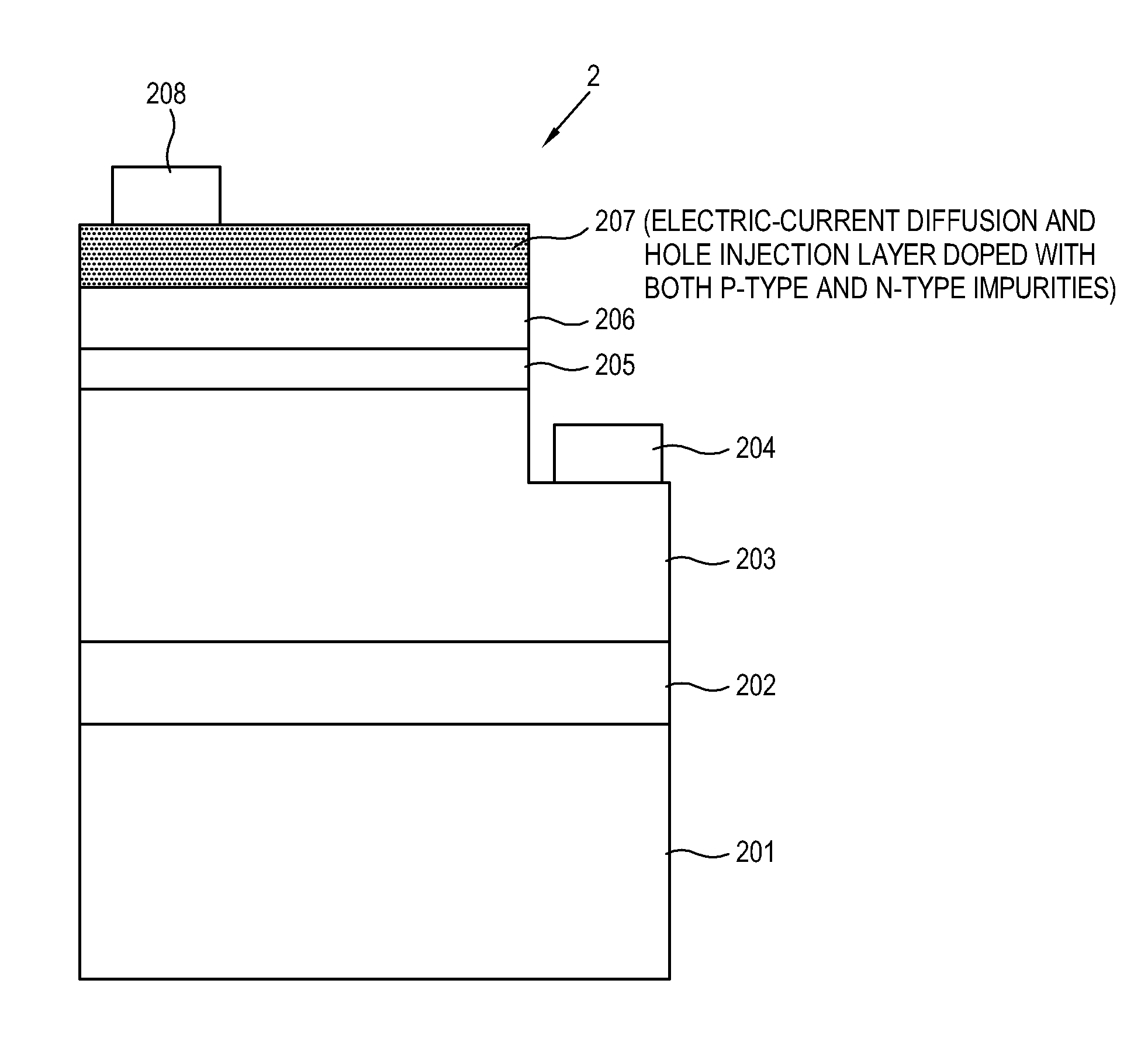
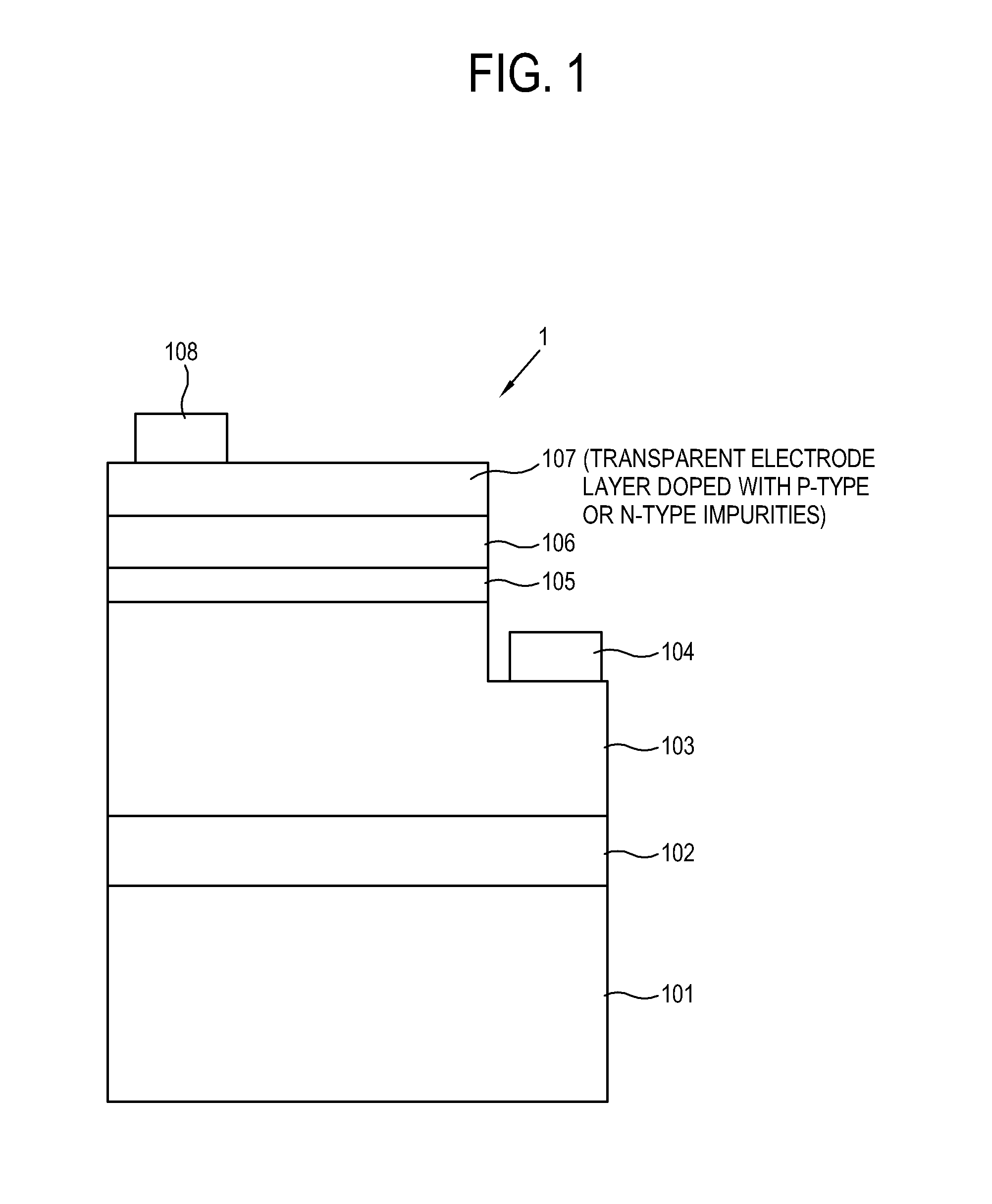
[0009]The foregoing and / or other aspects may be achieved by providing a semiconductor light emitting device including: a substrate; an n-type semiconductor layer giving an electron when receiving voltage; a p-type semiconductor layer giving a hole when receiving voltage; an active layer provided between the n-type semiconductor layer and the p-type semiconductor layer and including a quantum well structure to facilitate coupling between an electron and a hole; an n-type electrode including conductivity for applying voltage to the n-type semiconductor layer; a p-type electrode including conductivity for applying voltage to the p-type semiconductor layer; and am elect...


PUM


Abstract

Disclosed is a semiconductor light emitting device including: a substrate; an n-type semiconductor layer giving an electron when receiving voltage; a p-type semiconductor layer giving a hole when receiving voltage; an active layer provided between the n-type semiconductor layer and the p-type semiconductor layer and including a quantum well structure to facilitate coupling between an electron and a hole; an n-type electrode including conductivity for applying voltage to the n-type semiconductor layer; a p-type electrode including conductivity for applying voltage to the p-type semiconductor layer; and am electric-current diffusion and hole injection layer provided between the p-type semiconductor layer and the p-type electrode and doped with n-type impurities and p-type impurities for diffusing an electric current and injecting a hole between the p-type electrode and the p-type semiconductor layer. With this, ohmic contact is decreased, flow of an electric current is improved, diffusion of the electric current is more uniformized, and injection of a hole is improved between the electrode and the semiconductor layer of the semiconductor light emitting device, thereby maximizing efficiency of a device.

Description

TECHNICAL FIELD[0001]Apparatuses and methods consistent with the exemplary embodiments relate to a semiconductor light emitting device, and more particularly to a semiconductor light emitting device capable of enhancing diffusion of a current and injection of holes between an electrode and a semiconductor layer.BACKGROUND[0002]A semiconductor light emitting device, used in various fields such as a liquid crystal display (LCD) backlight, illumination, a display, etc. and widely known as a “light emitting diode (LED),” emits light on the principle that the light is emitted having a wavelength range corresponding to an energy gap between a conduction band and a valence band when a forward bias voltage is applied to a p-n junction semiconductor.[0003]Such a semiconductor light emitting device is required to be improved in various design indexes such as quantum efficiency, photon extraction efficiency, packaging, reliance, etc. Among such indexes, diffusion of an electric current and inj...

Claims


Application Information

Patent Timeline
Patent Type & Authority Applications(United States)
IPC IPC(8): H01L33/06
CPCH01L33/42H01L33/14
Inventor LEE, HAE-GWON
Owner QUANTUM DEVICES
Why Eureka
Try Eureka