Graphene Devices with Local Dual Gates

a graphene device and dual gate technology, applied in the field of local dual gate graphene devices, can solve the problems of poor fet leakage current and impracticality of large-scale complementary metal-oxide-semiconductor (cmos) transistors

Inactive Publication Date: 2012-07-12
IBM CORP
View PDF10 Cites 53 Cited by
  • Summary
  • Abstract
  • Description
  • Claims
  • Application Information

AI Technical Summary

Benefits of technology

[0006]For example, in a first aspect, a method of forming an electronic device comprises forming an insulator, embedding a local first gate in the insulator with a top surface of the first gate being substantially coplanar with a surface of the insulator, depositing a first dielectric layer over the first gate and insulator, and forming a channel comprising a bilayer graphene layer formed on the first dielectric layer. The first dielectric layer provides a flat surface on which the channel is formed. The method further comprises depositing a second dielectric layer over the bilayer graphene layer and forming a local second gate over the second dielectric layer. Each of the local first and second gates is capacitively coupled to the channel of the bilayer graphene layer. The local first and second gates form a first pair of gates to locally control a first portion of the bilayer graphene layer.
[0007]The method may further comprise forming a local third gate embedded in the insulator with a top surface of the third gate being substantially coplanar with a surface of the insulator and forming a local fourth gate over the second dielectric layer. Each of the local third and fourth gates is capacitively coupled to the channel of the bilayer graphene layer. The local third and fourth gates form at least a second pair of gates to locally control at least a second portion of the bilayer graphene layer. The at least second pair of gates operates as gates of a second transistor.
[0008]In a second aspect of the invention, an electronic device comprises an insulator, a local first gate embedded in the insulator with a top surface of the first gate being substantially coplanar with a surface of the insulator, a first dielectric layer formed over the first gate and insulator, and a channel comprising a bilayer graphene layer formed on the first dielectric layer. The first dielectric layer provides a substantially flat surface on which the channel is formed. The device further comprises a second dielectric layer formed over the bilayer graphene layer and a local second gate formed over the second dielectric layer. Each of the local first and second gates is capacitively coupled to the channel of the bilayer graphene layer. The local first and second gates form a first pair of gates to locally control a first portion of the bilayer graphene layer.
[0009]In a third aspect of the invention, an integrated circuit includes at least one dual gate graphene layer device circuit. The at least one device circuit comprises an insulator, a local first gate embedded in the insulator with a top surface of the first gate being substantially coplanar with a surface of the insulator, a first dielectric layer formed over the first gate and insulator, and a channel comprising a bilayer graphene layer formed on the first dielectric layer. The first dielectric layer provides a substantially flat surface on which the channel is formed. The device further comprises a second dielectric layer formed over the bilayer graphene layer and a local second gate formed over the second dielectric layer. Each of the local first and second gates is capacitively coupled to the channel of the bilayer graphene layer. The local first and second gates form a first pair of gates to locally control a first portion of the bilayer graphene layer.

Problems solved by technology

A free-standing graphene structure is theoretically stable only in a two-dimensional space, which implies that a planar graphene structure does not exist in a free state, being unstable with respect to formation of curved structures such as soot, fullerenes, and nanotubes.
Unfortunately, despite its high carrier mobility, grapheme has a zero band gap, which leads to a very poor FET leakage current.
However, the substrate structure makes large-scale complementary-metal-oxide-semiconductor (CMOS) transistor impractical due to the lack of threshold voltage (Vt) control of individual device.

Method used


Image

  • Graphene Devices with Local Dual Gates
  • Graphene Devices with Local Dual Gates
  • Graphene Devices with Local Dual Gates

Examples


Embodiment Construction

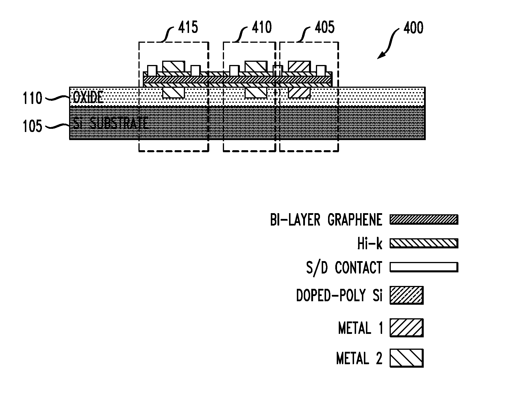
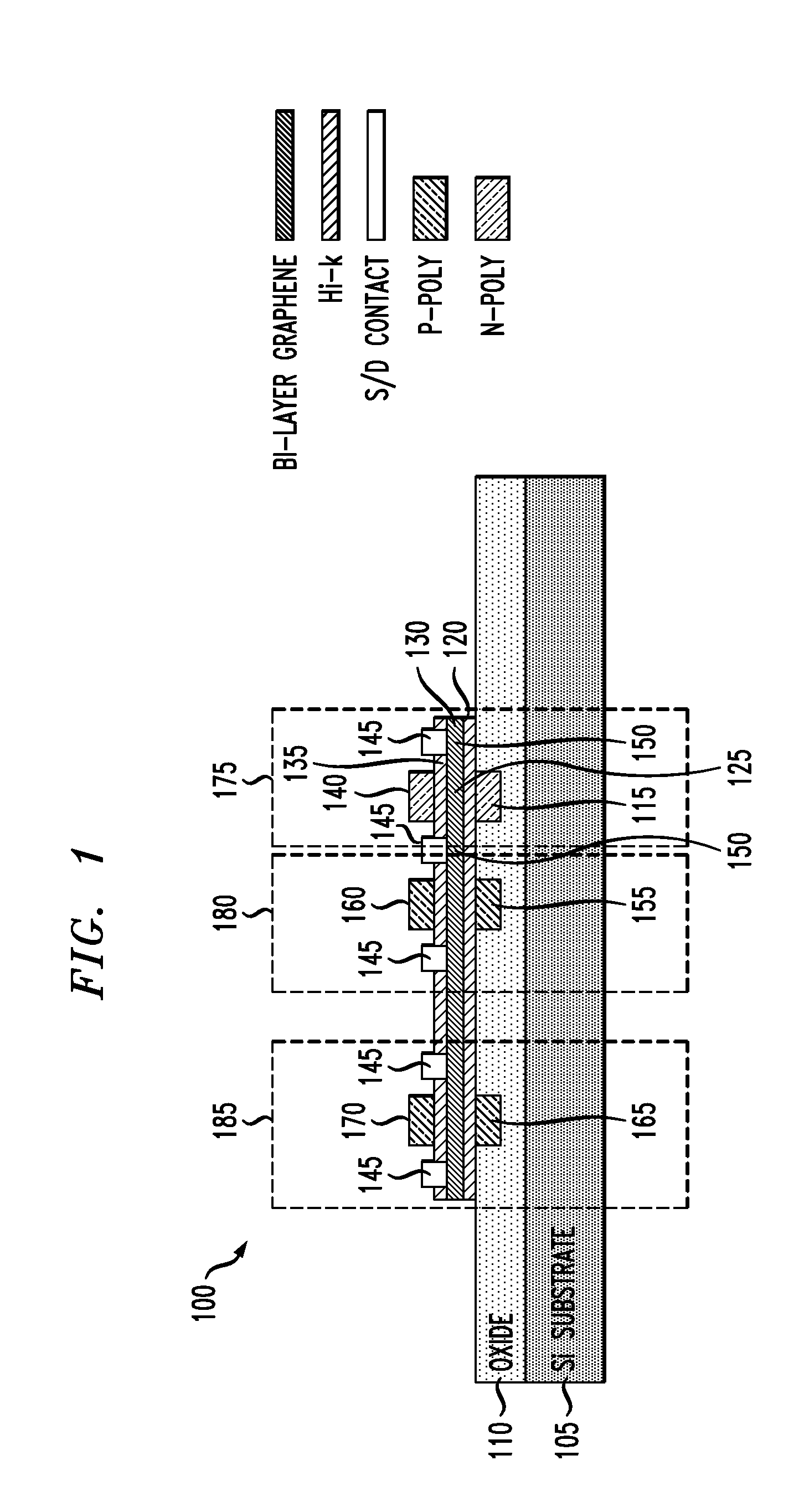
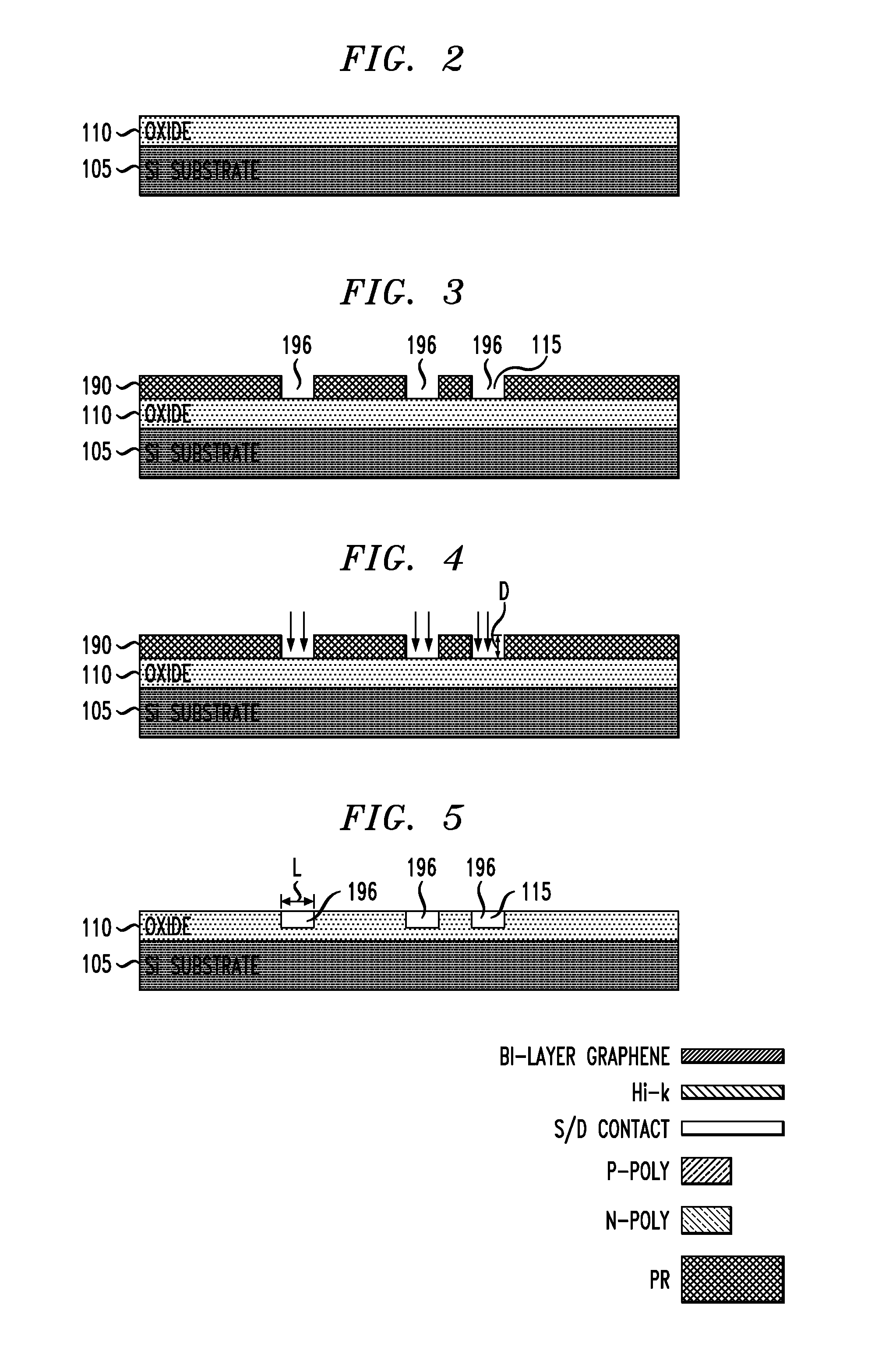
[0035]The present invention relates to graphene based electronic device, such as a field-effect transistor (FET) and methods of manufacturing the same. Graphene's bilayer electronic band structure has led to an interest of creating tunable band gap bilayer electronic devices such as a FET. In manufacturing of electronic devices, typically a wafer can hold multiple devices. The electronic device discussed herein includes a patterned top and bottom gates to bias different voltages on different devices on the same wafer to different band gap or threshold voltage (Vt) depending on the device and / or circuit requirement. An advantage of using a patterned bottom gate is the ability to form CMOS logic devices and / or technologies with multiple device Vt offerings, which is common in today's semiconductor industry. For example, low Vt devices for high switching speed and high Vt devices for low power are usually provided on the same wafer.

[0036]Besides the lack of controllability of individua...


PUM


Abstract

An electronic device comprises an insulator, a local first gate embedded in the insulator with a top surface of the first gate being substantially coplanar with a surface of the insulator, a first dielectric layer formed over the first gate and insulator, and a channel. The channel comprises a bilayer graphene layer formed on the first dielectric layer. The first dielectric layer provides a substantially flat surface on which the channel is formed. A second dielectric layer formed over the bilayer graphene layer and a local second gate formed over the second dielectric layer. Each of the local first and second gates is capacitively coupled to the channel of the bilayer graphene layer. The local first and second gates form a first pair of gates to locally control a first portion of the bilayer graphene layer.

Description

FIELD OF THE INVENTION[0001]The present invention relates to semiconductor structures, and particularly to local dual gates graphene based devices and methods of manufacturing the same.BACKGROUND OF THE INVENTION[0002]In a semiconductor material, band gap is an important parameter, which to a large extent determines properties of the semiconductor material. The band gap is defined as the difference in energy between the top of the valence band and the bottom of the conduction band. This is the energy that is required to excite an electron from the valence band into the conduction band. Electrons in the conduction band have the ability to move through the material, thereby enabling conduction of electricity.[0003]One type of semiconductor material, graphene, is of great interest for nanoscale electronics due to the much higher carrier mobility compared to Silicon. Graphene is a two-dimensional planar sheet of carbon atoms arranged in a hexagonal benzene-ring structure. A free-standin...

Claims


Application Information

Patent Timeline
Patent Type & Authority Applications(United States)
IPC IPC(8): H01L29/15H01L21/336
CPCH01L29/4908H01L29/66742H01L29/1606H01L29/78684H01L29/66015H01L29/78648H01L21/00H01L21/84H01L29/66045H01L29/4916H01L29/517H01L21/02527H01L21/044H01L29/42384H01L29/42376H01L21/02178H01L21/02181H01L29/78645
Inventor CHEN, ZHIHONGFRANKLIN, AARON DANIELHAN, SHU-JEN
Owner IBM CORP
Why Eureka
Try Eureka