Semiconductor processing system and methods using capacitively coupled plasma

a processing system and capacitively coupled technology, applied in the field of semiconductor processing system and capacitively coupled plasma, can solve the problems of reducing the etching rate, affecting the material's performance, and creating fabrication challenges, so as to improve the control of the environment, reduce or eliminate the number of ionically charged species, and precise control of the etching rate

Inactive Publication Date: 2012-07-19
APPLIED MATERIALS INC
View PDF5 Cites 525 Cited by
  • Summary
  • Abstract
  • Description
  • Claims
  • Application Information

AI Technical Summary

Benefits of technology

[0006]Systems and methods are described for improved control of the environment between a plasma and the surfaces of a substrate wafer that are exposed to plasma and / or its effluents. The improved control may be realized at least in part by an ion suppression element positioned between the plasma and the substrate that reduces or eliminates the number of ionically-charged species that reach the substrate. Adjusting the concentration of ion species that reach the substrate surface allows more precise control of the etch rate, etch selectivity, and deposition chemistry (among other parameters) during a plasma assisted etch and / or deposition on the substrate.
[0007]In some examples, the ion suppression element may be part of the gas / precursor delivery equipment of a substrate processing chamber. For example, a showerhead positioned inside the chamber between a plasma region and the substrate may act as both a distribution component for gases and precursors as well as an ion suppressor that reduces the amount of ionized species traveling through the showerhead from the plasma region to the substrate. In additional examples, the ion suppression element may be a partition between the plasma region and the substrate that has one or more openings through which plasma effluents may pass from the plasma region to the substrate. The size, position and geometry of the openings, the distance between the partition and the substrate, and the electrical bias on the partition, among other characteristics, may be selected to control the amounts of charged species reaching the substrate. In some instances the partition may also act as an electrode that helps generate and define the plasma region in the processing chamber.

Problems solved by technology

While plasma environments are generally less destructive to substrates than high-temperature deposition environments, they still create fabrication challenges.
Etching precision can be a problem with energetic plasmas that over-etch shallow trenches and gaps.
Energetic species in the plasmas, especially ionized species, can create unwanted reactions in a deposited material that adversely affect the material's performance.

Method used


Image

  • Semiconductor processing system and methods using capacitively coupled plasma
  • Semiconductor processing system and methods using capacitively coupled plasma
  • Semiconductor processing system and methods using capacitively coupled plasma

Examples


Embodiment Construction

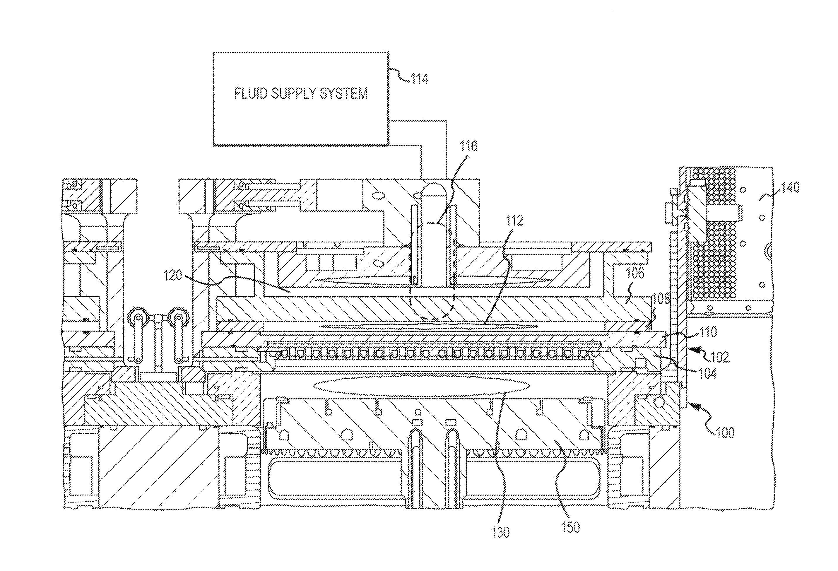
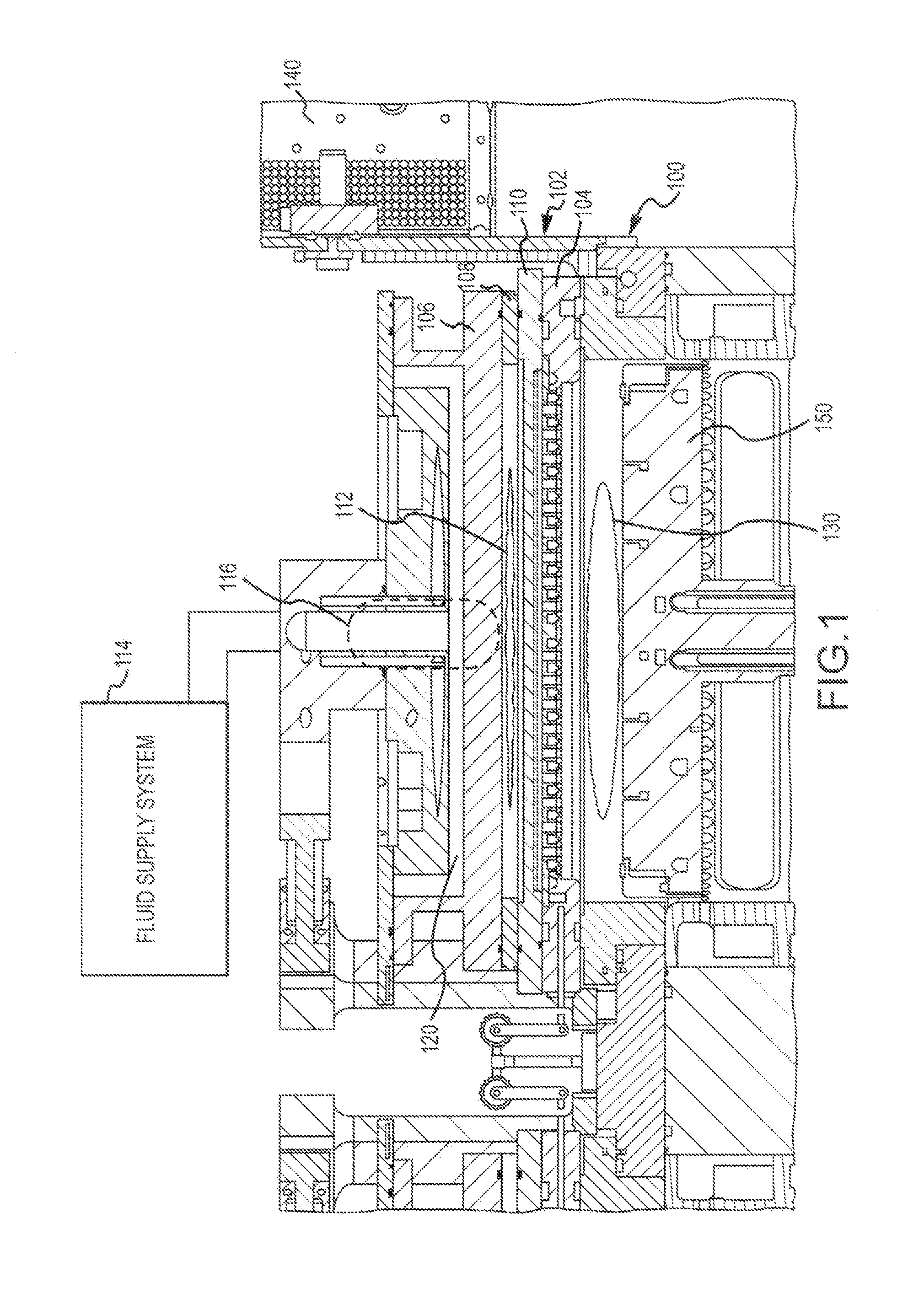
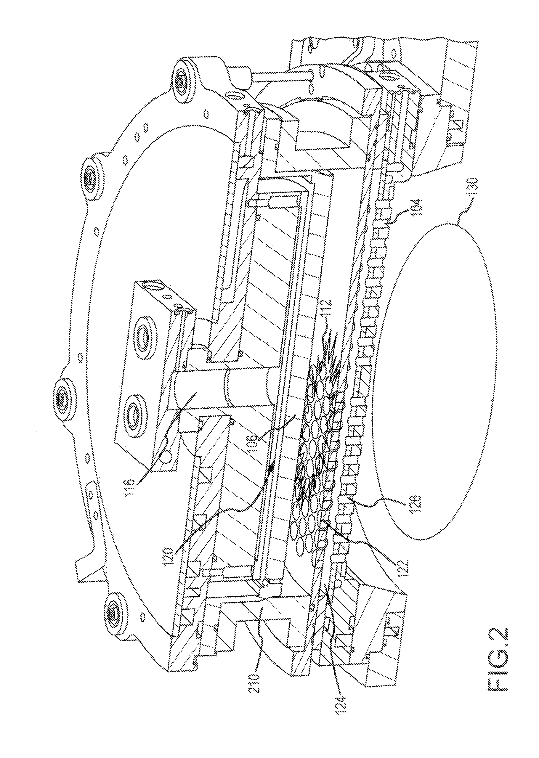
[0023]Systems and methods are described for the generation and control of a plasma inside a semiconductor processing chamber. The plasma may originate inside the processing chamber, outside the processing chamber in a remote plasma unit, or both. Inside the chamber, the plasma is contained and separated from the substrate wafer with the help of an ion suppression element that is positioned between the plasma and the substrate wafer. In some instances, this ion suppression element may also function as part of a plasma generation unit (e.g., an electrode), a gas / precursor distribution system (e.g., a showerhead), and / or another component of the processor system. In additional instances, the ion suppression element may function primarily to define a partition between a plasma generation region and a gas reaction region that etches and / or deposits material on exposed surfaces of the substrate wafer.

[0024]The ion suppression element functions to reduce or eliminate the amount of ionicall...


PUM

PropertyMeasurementUnit
pressureaaaaaaaaaa
temperaturesaaaaaaaaaa

Abstract

Substrate processing systems are described that have a capacitively coupled plasma (CCP) unit positioned inside a process chamber. The CCP unit may include a plasma excitation region formed between a first electrode and a second electrode. The first electrode may include a first plurality of openings to permit a first gas to enter the plasma excitation region, and the second electrode may include a second plurality of openings to permit an activated gas to exit the plasma excitation region. The system may further include a gas inlet for supplying the first gas to the first electrode of the CCP unit, and a pedestal that is operable to support a substrate. The pedestal is positioned below a gas reaction region into which the activated gas travels from the CCP unit.

Description

CROSS-REFERENCES TO RELATED APPLICATIONS[0001]This application is a nonprovisional of, and claims the benefit of the filing date of, U.S. Provisional Patent Application No. 61 / 433,633, entitled “SEMICONDUCTOR PROCESSING SYSTEM AND METHODS USING CAPACITIVELY COUPLED PLASMA, filed Jan. 18, 2011, the entire disclosure of which is incorporated herein by reference for all purposes.BACKGROUND OF THE INVENTION[0002]Plasma deposition and etching processes for fabricating semiconductor integrated circuits have been in wide use for decades. These processes typically involve the formation of a plasma from plasma-generating gases that are exposed to electric fields of sufficient power inside the processing chamber to cause the gases to ionize. The temperatures needed to form these gases into plasmas can be much lower than needed to thermally ionize the same gases. Thus, plasma generation processes can be used to generate reactive radical and ion species from the starting gases at significantly ...

Claims


Application Information

Patent Timeline
Patent Type & Authority Applications(United States)
IPC IPC(8): C23F1/02C23C16/458C23C16/455C23C16/50
CPCC23C16/45565H01J37/32091H01J37/32357H05H1/24H01J37/3244H01J37/32724H01J37/32422H01L21/205H01L21/3065C23C16/45585H01L21/02274H01J37/32532H01J37/32541H01J37/32568H01J37/32449
Inventor YANG, JANG-GYOOMILLER, MATTHEW L.CHEN, XINGLONGCHUC, KIEN N.LIANG, QIWEIVENKATARAMAN, SHANKARLUBOMIRSKY, DMITRY
Owner APPLIED MATERIALS INC
Why Eureka
Try Eureka