Al technical title is built by PatSnap Al team. It summarizes the technical point description of the patent document.
a technology for semiconductor devices and packaging, applied in semiconductor devices, semiconductor/solid-state device details, electrical devices, etc., can solve the problems of difficult to stop partial etching of metal rolls with sufficient accuracy and repeatability, and add to the cost of manufacturing devices, so as to facilitate the fabrication of packages and limit the spread of adhesive materials
Inactive Publication Date: 2012-07-19
GEM SERVICES
View PDF11 Cites 27 Cited by
Summary
Abstract
Description
Claims
Application Information
AI Technical Summary
This helps you quickly interpret patents by identifying the three key elements:
Problems solved by technology
Method used
Benefits of technology
[0014]Embodiments of the present invention relate to the use of stamping to form features on a lead frame of a semiconductor device package. In one embodiment, portions of the lead frame such as pins are moved out of the horizontal plane of a diepad by stamping. In certain embodiments, a complex cross-sectional profile, such as chamfered, may be imparted to portions of the pins and / or diepad by stamping. The complexity offered by such a stamped cross-sectional profile serves to enhance mechanical interlocking of the lead frame within the plastic molding of the package body. Other techniques such as selective electroplating and / or formation of a brown oxide guard band to limit spreading of adhesive material during die attach, may be employed alone or in combination to facilitate fabrication of a package having such stamped features.
Problems solved by technology
While the conventional process flow just described is adequate to form a semiconductor device package, it may offer certain drawbacks.
In particular, the partial etching step shown in FIG. 1C may be difficult to achieve, and hence adds to the cost of manufacturing the device.
In particular, the partial etching of the metal roll may be difficult to halt with sufficient accuracy and repeatability.
Method used
Image
Click on the blue label to locate the original text in one second.
Reading with bidirectional positioning of images and text.
Examples
Embodiment Construction
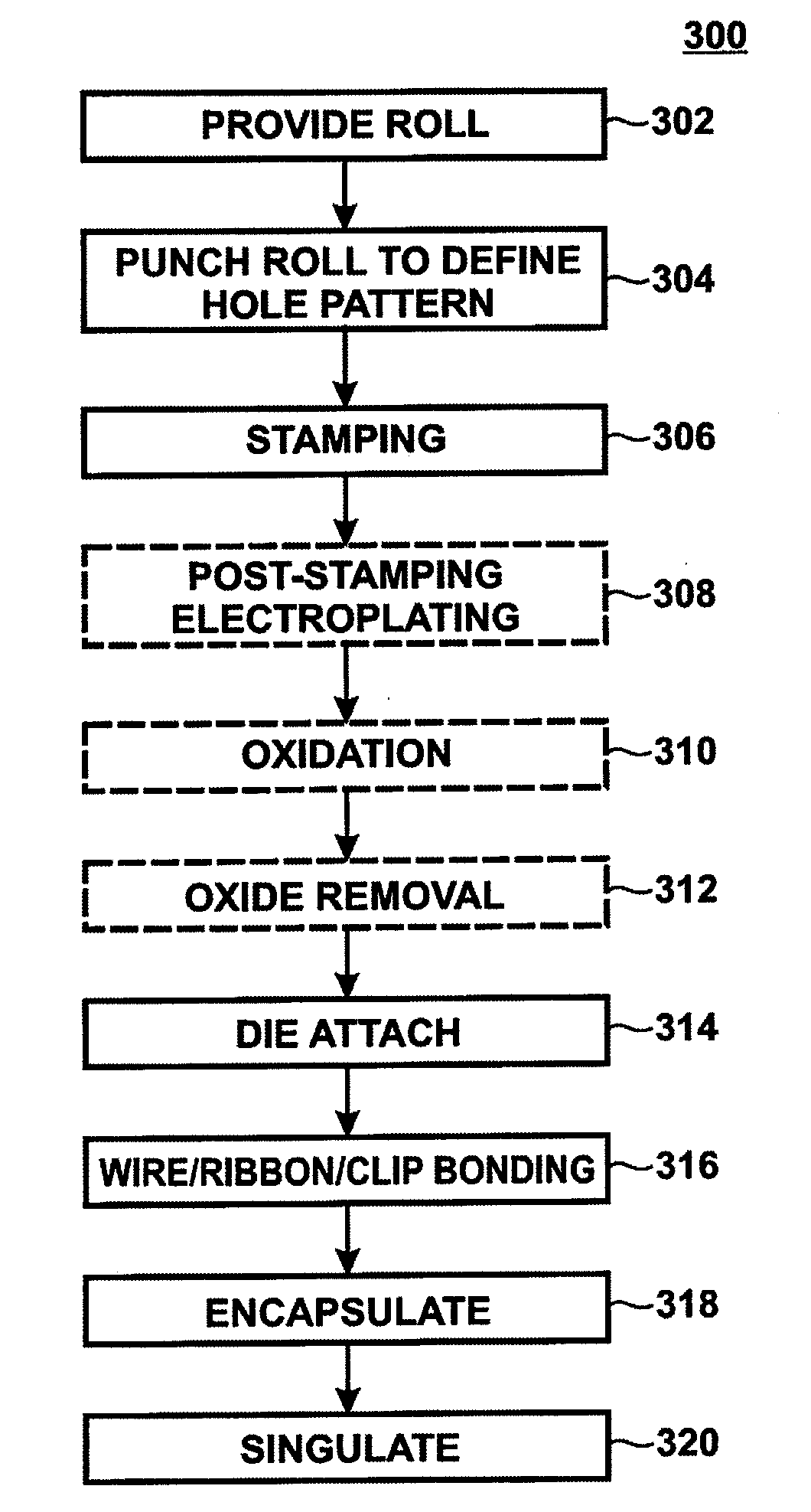
[0057]Embodiments of the present invention relate to the formation of semiconductor device packages utilizing stamping. In one embodiment, portions of the lead frame such as pins are moved out of the horizontal plane of a diepad by stamping. In certain embodiments, the pins of a package may be imbued with a chamfered or other complex cross-sectional profile by a stamping process. Other techniques, employed alone or in combination, may facilitate fabrication of a package by stamping.
[0058]FIGS. 2A-2K show simplified cross-sectional views of a process in accordance with an embodiment of the present invention for forming a semiconductor device package. The views of FIGS. 2A-2K are simplified in that the relative proportions of the components of the package are not shown to scale.
[0059]In FIG. 2A, a planar, continuous roll 202 of conducting material such as copper, is provided. In particular embodiments, the metal roll may have a thickness of between about 4-20 mils (0.004″-0.020″). In ...
PUM
Abstract
Embodiments of the present invention relate to the use of stamping to form features on a lead frame of a semiconductor device package. In one embodiment, portions of the lead frame such as pins are moved out of the horizontal plane of a diepad by stamping. In certain embodiments, indentations or a complex cross-sectional profile, such as chamfered, may be imparted to portions of the pins and / or diepad by stamping. The complexity offered by such a stamped cross-sectional profile serves to enhance mechanical interlocking of the lead frame within the plastic molding of the package body. Other techniques such as selective electroplating and / or formation of a brown oxide guard band to limit spreading of adhesive material during die attach, may be employed alone or in combination to facilitate fabrication of a package having such stamped features.
Description
CROSS-REFERENCE TO RELATED APPLICATION[0001]This application is a continuation-in-part of U.S. patent application Ser. No. 12 / 186,342, filed Aug. 5, 2008, by Tsui et al., which claims priority to the U.S. Provisional Patent Application No. 61 / 053,561, filed May 15, 2008, both of which are incorporated by reference in their entirety herein for all purposes.[0002]This application is also a continuation-in-part of U.S. patent application Ser. No. 12 / 903,626, filed Oct. 13, 2010, by Tsui et al., which is a division of U.S. patent application Ser. No. 12 / 191,527, filed Aug. 14, 2008, which issued as U.S. Pat. No. 7,838,339 on Nov. 23, 2010, which claims priority to U.S. Provisional Application No. 61 / 042,602 filed Apr. 4, 2008, all of which are incorporated by reference in their entirety herein for all purposes.BACKGROUND OF THE INVENTION[0003]FIGS. 1A-1H show simplified cross-sectional views of a conventional process for fabricating a package for a semiconductor device. The views of FIG...
Claims
Application Information
Patent Timeline
Application Date:The date an application was filed.
Publication Date:The date a patent or application was officially published.
First Publication Date:The earliest publication date of a patent with the same application number.
Issue Date:Publication date of the patent grant document.
PCT Entry Date:The Entry date of PCT National Phase.
Estimated Expiry Date:The statutory expiry date of a patent right according to the Patent Law, and it is the longest term of protection that the patent right can achieve without the termination of the patent right due to other reasons(Term extension factor has been taken into account ).
Invalid Date:Actual expiry date is based on effective date or publication date of legal transaction data of invalid patent.
Patent Type & Authority Applications(United States)