Semiconductor device and semiconductor memory device
- Summary
- Abstract
- Description
- Claims
- Application Information
AI Technical Summary
Benefits of technology
Problems solved by technology
Method used
Image

Examples
embodiment 1
[0033]In this embodiment, an example of a semiconductor device that includes a memory circuit capable of storing data for a certain period is described.
[0034]Note that a memory circuit is a circuit capable of retaining electric charge as data for a certain period.
[0035]The example of the semiconductor device in this embodiment includes a memory circuit.
[0036]An example of the memory circuit is described with reference to FIGS. 1A to 1F.
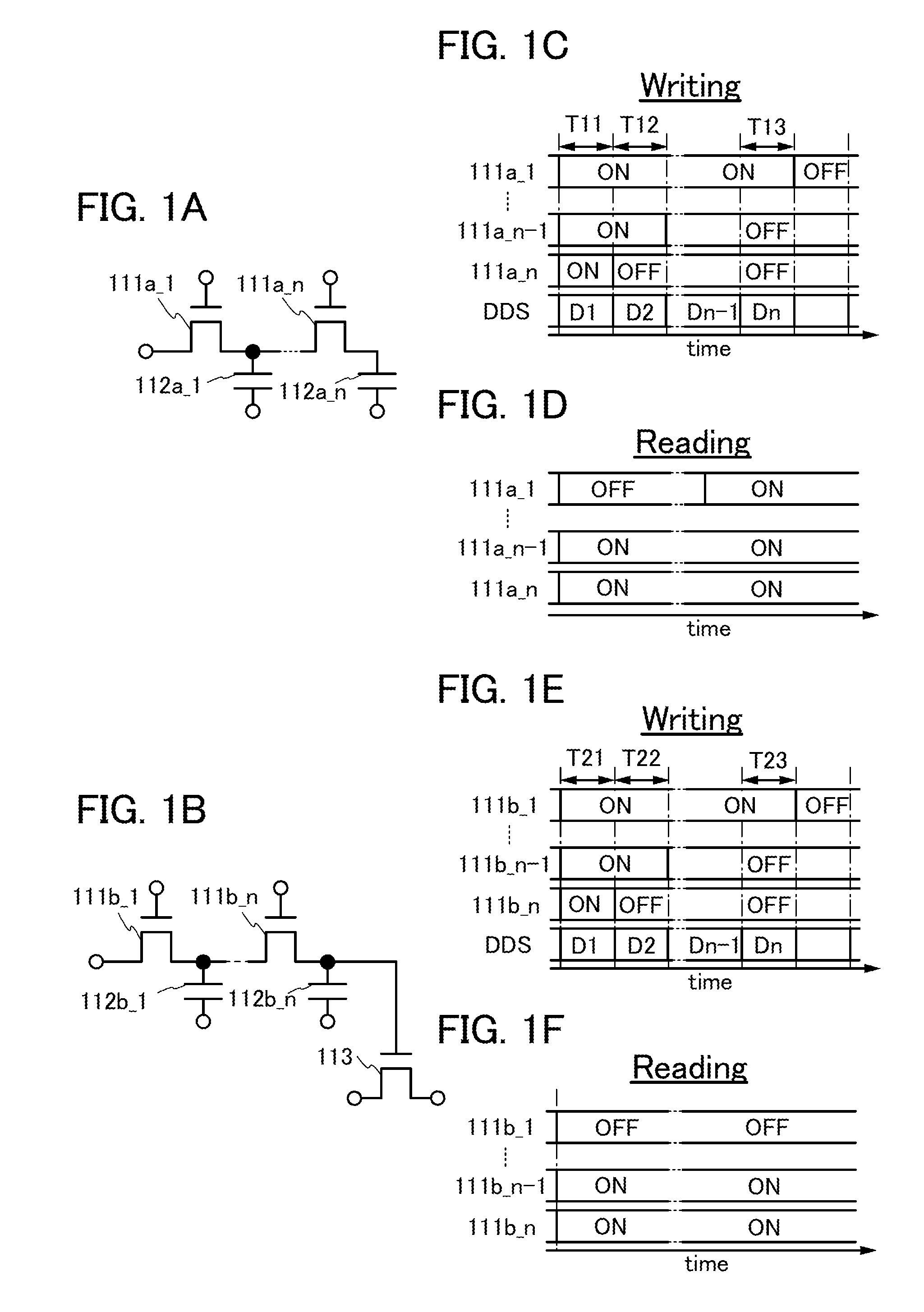
[0037]First, examples of a structure of the memory circuit in the semiconductor device in this embodiment are described with reference to FIGS. 1A and 1B. FIGS. 1A and 1B are circuit diagrams illustrating examples of the structure of the memory circuit in this embodiment.
[0038]The memory circuit illustrated in FIG 1A includes n transistors 111a (transistors 111a_1 to 111a_n) (n is a natural number of 2 or more), and n capacitors 112a (capacitors 112a_1 to 112a_n).
[0039]Note that the transistor includes two terminals and a current control terminal for ...
embodiment 2
[0101]In this embodiment, an example of a semiconductor memory device is described as an example of the semiconductor device in the above embodiment.
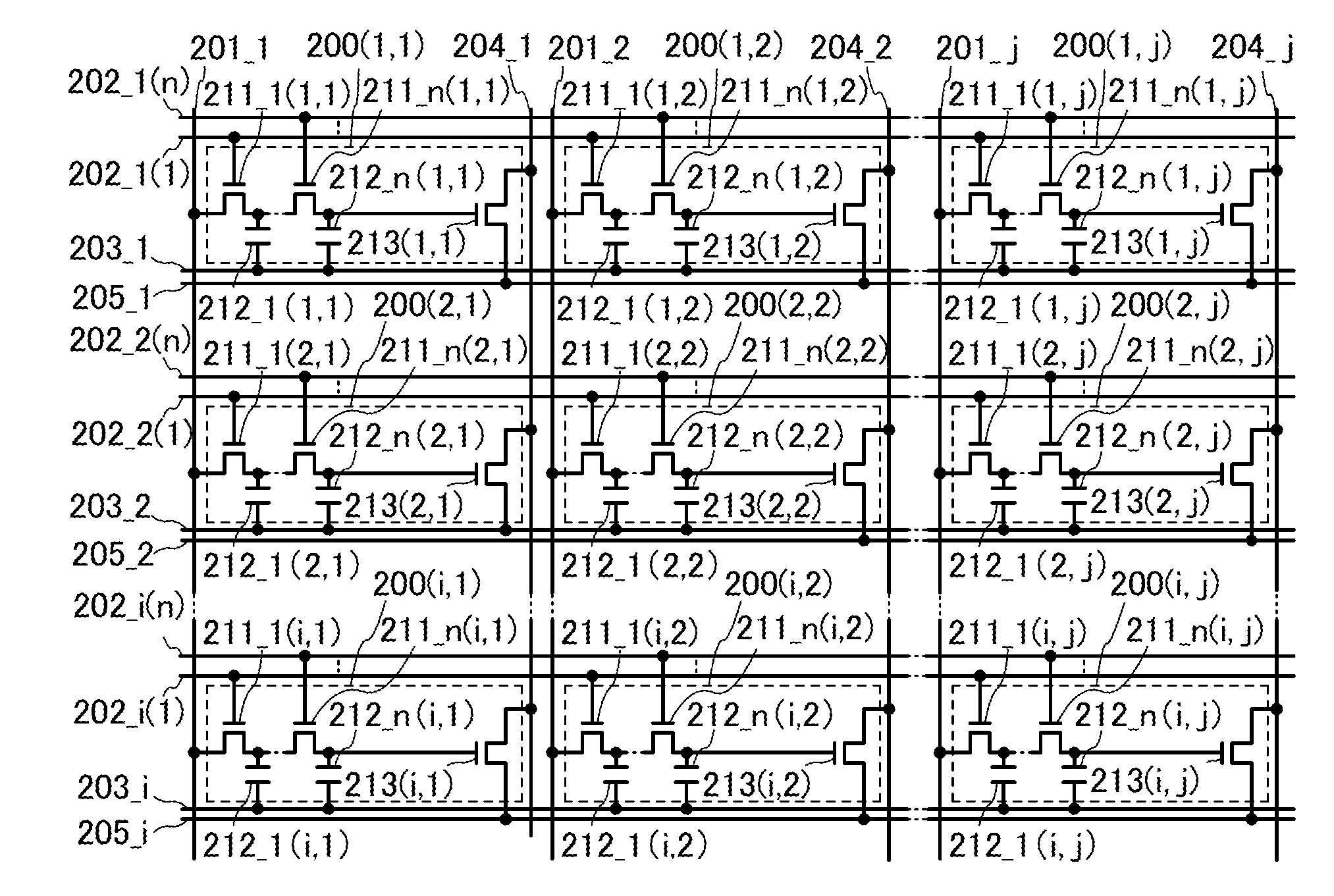
[0102]An example of a semiconductor memory device in this embodiment includes a memory cell array including a plurality of memory cells arranged in a matrix of i rows (i is a natural number of 2 or more) and j columns (j is a natural number). The memory cell corresponds to the memory circuit in the semiconductor device in the above embodiment.
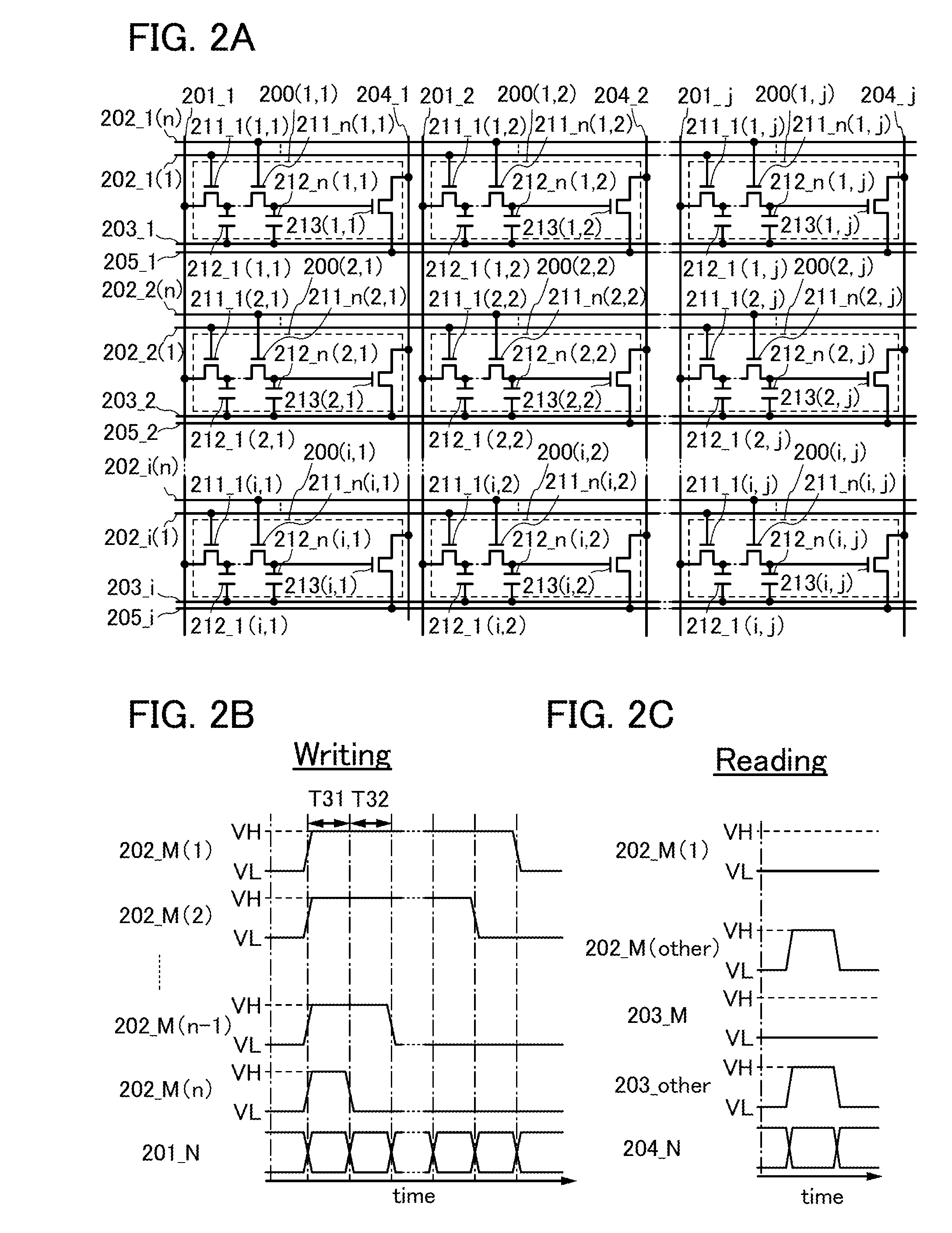
[0103]An example of the memory cell array in the semiconductor memory device in this embodiment is described with reference to FIGS. 2A to 2C.
[0104]First, an example of the circuit structure of the memory cell array in the semiconductor memory device in this embodiment is described with reference to FIG. 2A.
[0105]A memory cell array illustrated in FIG. 2A includes a plurality of memory cells 200 arranged in a matrix of i rows and j columns; j wirings 201 (wirings 201_1 to 201_j); i×n wirings 202 (n...
embodiment 3
[0146]In this embodiment, an example of a transistor including an oxide semiconductor layer which can be used for a semiconductor device or a semiconductor memory device in the above embodiment is described.
[0147]Examples of structures of the transistors in this embodiment are described with reference to FIGS. 4A to 4D. FIGS. 4A to 4D are cross-sectional schematic views each illustrating an example of a structure of a transistor in this embodiment. Note that the components illustrated in FIGS. 4A to 4D include those having sizes different from the actual sizes.
[0148]A transistor illustrated in FIG. 4A is one of top-gate transistors.
[0149]The transistor illustrated in FIG. 4A includes a semiconductor layer 603_A, a conductive layer 605a_A, a conductive layer 605b_A, an insulating layer 606_A, and a conductive layer 607_A.
[0150]The semiconductor layer 603_A includes a region 604a_A and a region 604b_A that are regions which are separated from each other and to which a dopant is added....
PUM
 Abstract
Description
Claims
Application Information
 - R&D Engineer
- R&D Manager
- IP Professional
- Industry Leading Data Capabilities
- Powerful AI technology
- Patent DNA Extraction
Browse by: Latest US Patents, China's latest patents, Technical Efficacy Thesaurus, Application Domain, Technology Topic.
© 2024 PatSnap. All rights reserved.Legal|Privacy policy|Modern Slavery Act Transparency Statement|Sitemap