

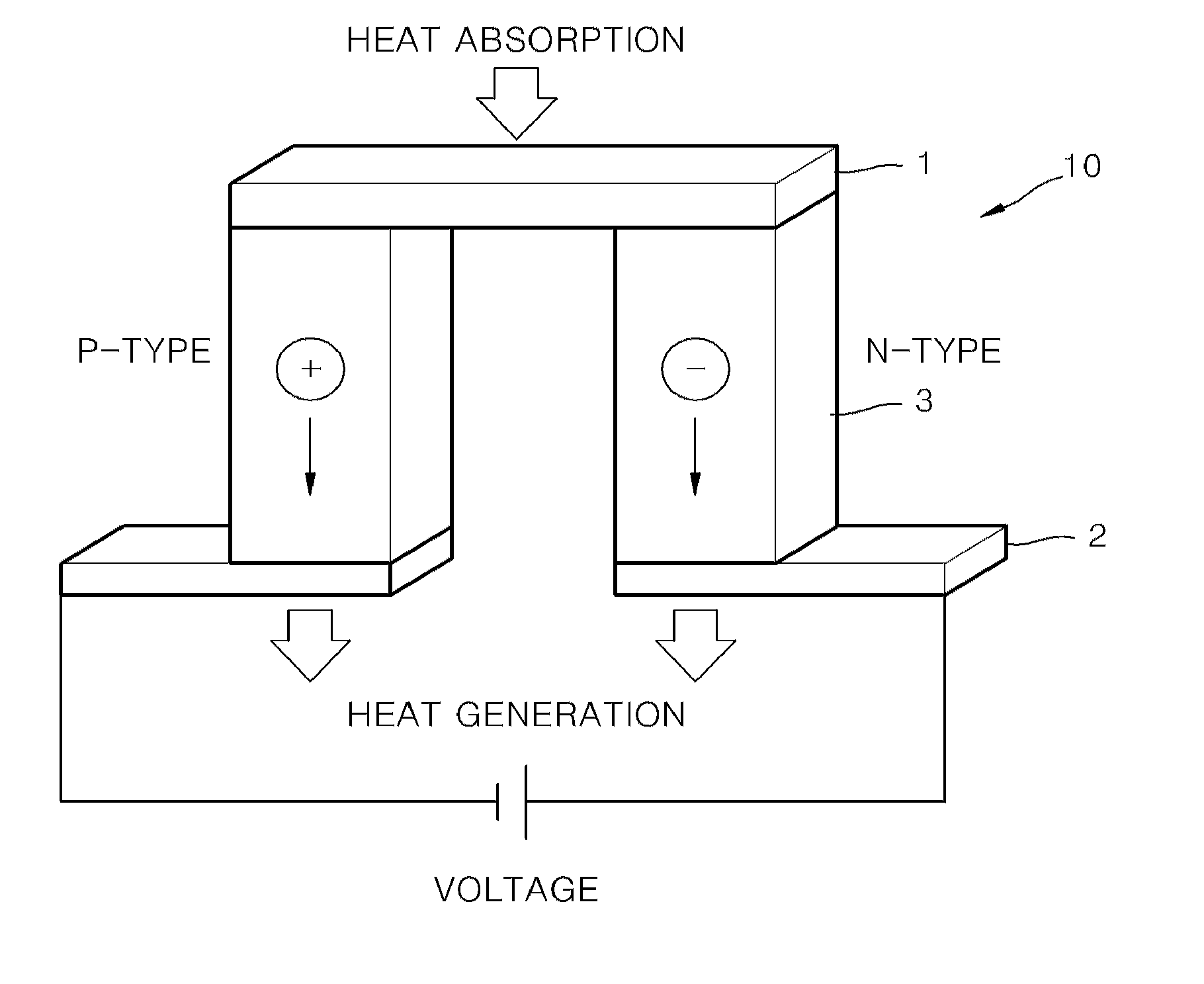
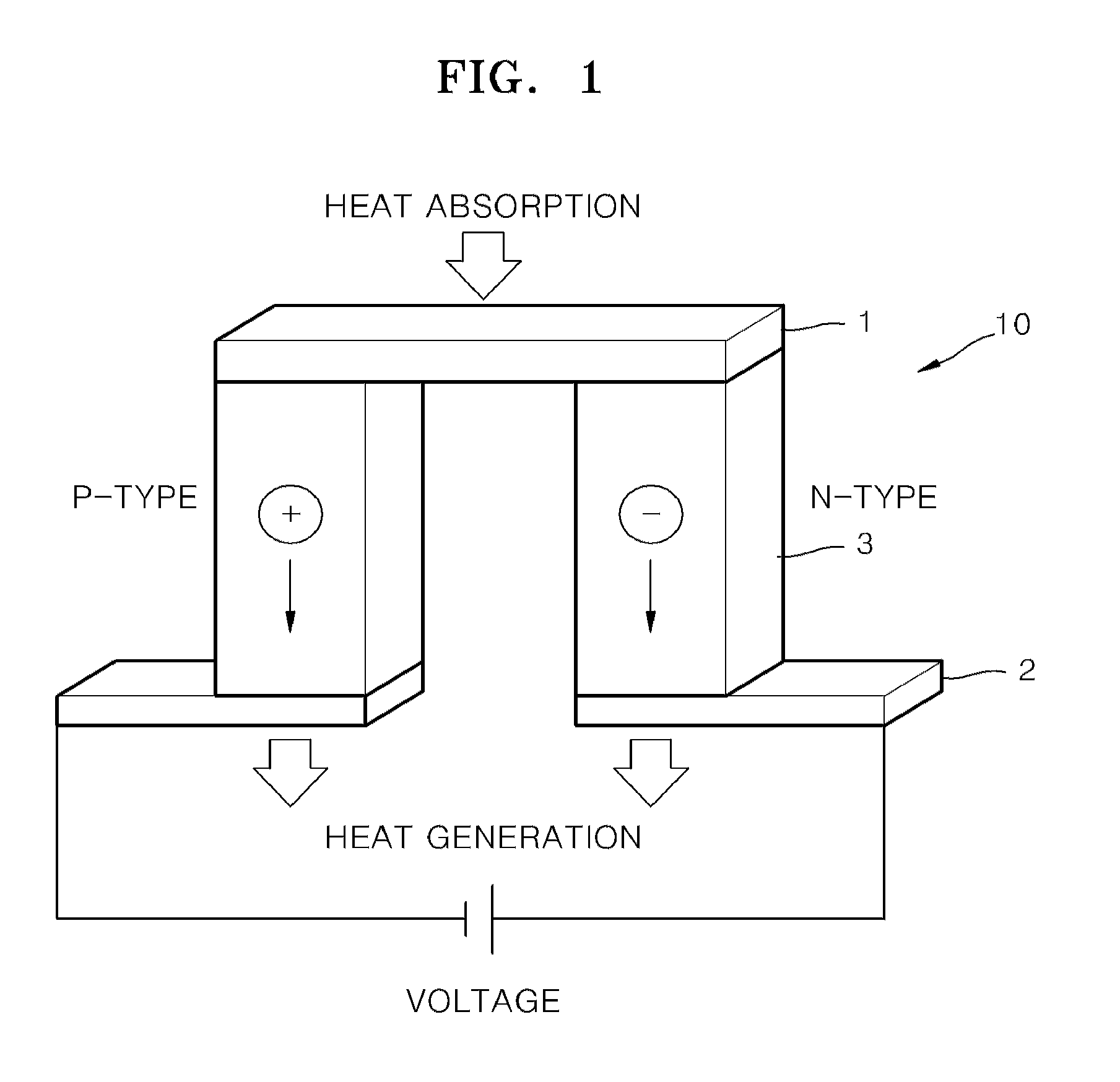
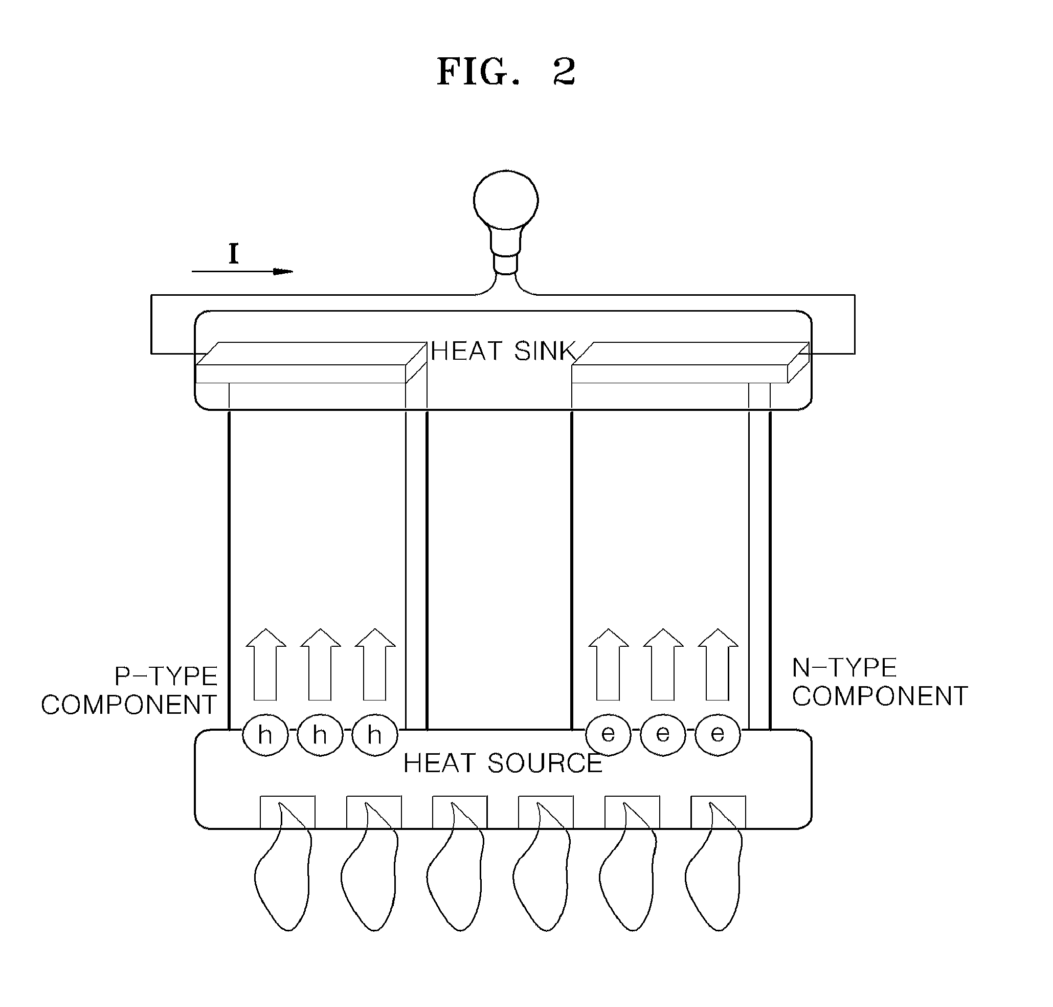
Thermoelectric material including nanoinclusions, thermoelectric module and thermoelectric apparatus including the same
a technology of thermoelectric modules and thermoelectric devices, applied in non-metal conductors, conductors, transportation and packaging, etc., can solve the problems of inability to quickly solve heat generation problems and demand for active cooling, and achieve the effect of improving thermoelectric conversion efficiency
- Summary
- Abstract
- Description
- Claims
- Application Information
AI Technical Summary
Benefits of technology
Problems solved by technology
Method used
Image

Examples
examples 1 to 4
[0094]Multi-Target Pulsed Laser Deposition (“MTPLD”), which is a type of physical vapor deposition, was used to prepare a thermoelectric material into which nano-inclusions are inserted. A MgO substrate having the dimensions 10 millimeters (mm) X 5 mm×0.5 mm of MgO 100 was used as a substrate. The target for deposition of the thermoelectric material had a composition of Bi0.5Sb1.5Te3. A Te target was used for deposition of nano-inclusions. The MTPLD was performed using a 2 joule per square centimeter (J / cm) of KrF 248 nm Excimer Laser at 125° C. and 200 milliTorr (mTorr) of argon partial pressure. Annealing was performed at 225° C. for 2 hours.
[0095]The total thickness of the each of the thermoelectric materials of Examples 1 to 4 was about 500 nm. Each of the thermoelectric materials of Examples 1 to 4 included Bi0.5Sb1.5Te3 (“BST”) and Te, and a total amount of Te in Examples 1, 2, 3, and 4 was about 2.5 volume percent (vol %), about 5 vol %, 7.5 vol %, and 15 vol %, respectively....
experimental example 1
[0101]Seebeck coefficients and electrical conductivities of the thermoelectric materials prepared in Examples 1 to 4 and Comparative Example 1 were measured using a ZEM-3 from ULVAC-RIKO, Inc. (Japan), and a power factor was calculated based on a result of the measurement of the Seebeck coefficients and the electrical conductivities of the thermoelectric materials. The results are shown in FIGS. 6A, 6B, 7A, 7B, 8A, and 8B.
[0102]As shown in FIG. 6A, Seebeck coefficients in the materials of Examples 1 to 4, which include Te nano-inclusions, were increased by about 9% to about 45% as compared to the Seebeck coefficient of the material of Comparative Example 1 (based on 320K data). Also, as shown in FIG. 6B, the Seebeck coefficients of the materials of Examples 1 to 4, which include Te nano-inclusions, were increased as the amount of nano-inclusions increased.
[0103]As shown in FIG. 7A, the electrical conductivity of the materials of Examples 1 to 4 tends to decreased by about 2% to abou...
PUM
| Property | Measurement | Unit |
|---|---|---|
| average particle diameter | aaaaa | aaaaa |
| distance | aaaaa | aaaaa |
| total thickness | aaaaa | aaaaa |
Abstract
Description
Claims
Application Information