Radiation-Emitting Semiconductor Component

a technology of semiconductor components and radiation, applied in the direction of semiconductor devices, basic electric elements, electrical appliances, etc., can solve the problems of unfavorable distribution of the resulting emission color, and achieve the effect of being used particularly efficiently

Inactive Publication Date: 2012-08-02
OSRAM OPTO SEMICONDUCTORS GMBH
View PDF3 Cites 30 Cited by
  • Summary
  • Abstract
  • Description
  • Claims
  • Application Information

AI Technical Summary

Benefits of technology

[0036]In accordance with at least one embodiment of the radiation-emitting semiconductor component, at least one conductor track for making contact with at least one of the emission regions of the light-emitting diode chip is arranged below at least one emission area. This embodiment has the advantage, inter alia, that the first main...

Problems solved by technology

In practice, firstly the wavelengths of the primary radiation from different light-emitting diode chips differ, even if the latter are produced jointly and originate from a single wafer, for example, and secondly the optical thicknesses of t...

Method used


Image

  • Radiation-Emitting Semiconductor Component
  • Radiation-Emitting Semiconductor Component
  • Radiation-Emitting Semiconductor Component

Examples


Embodiment Construction

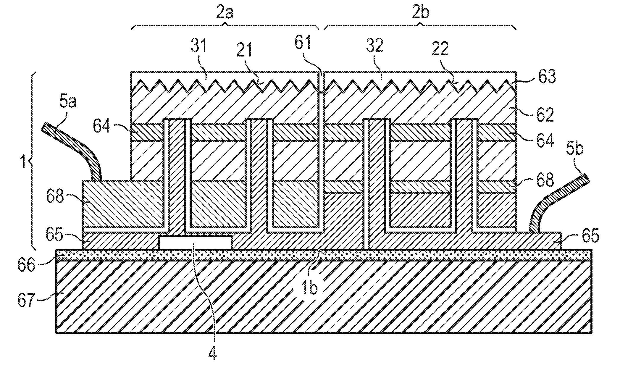
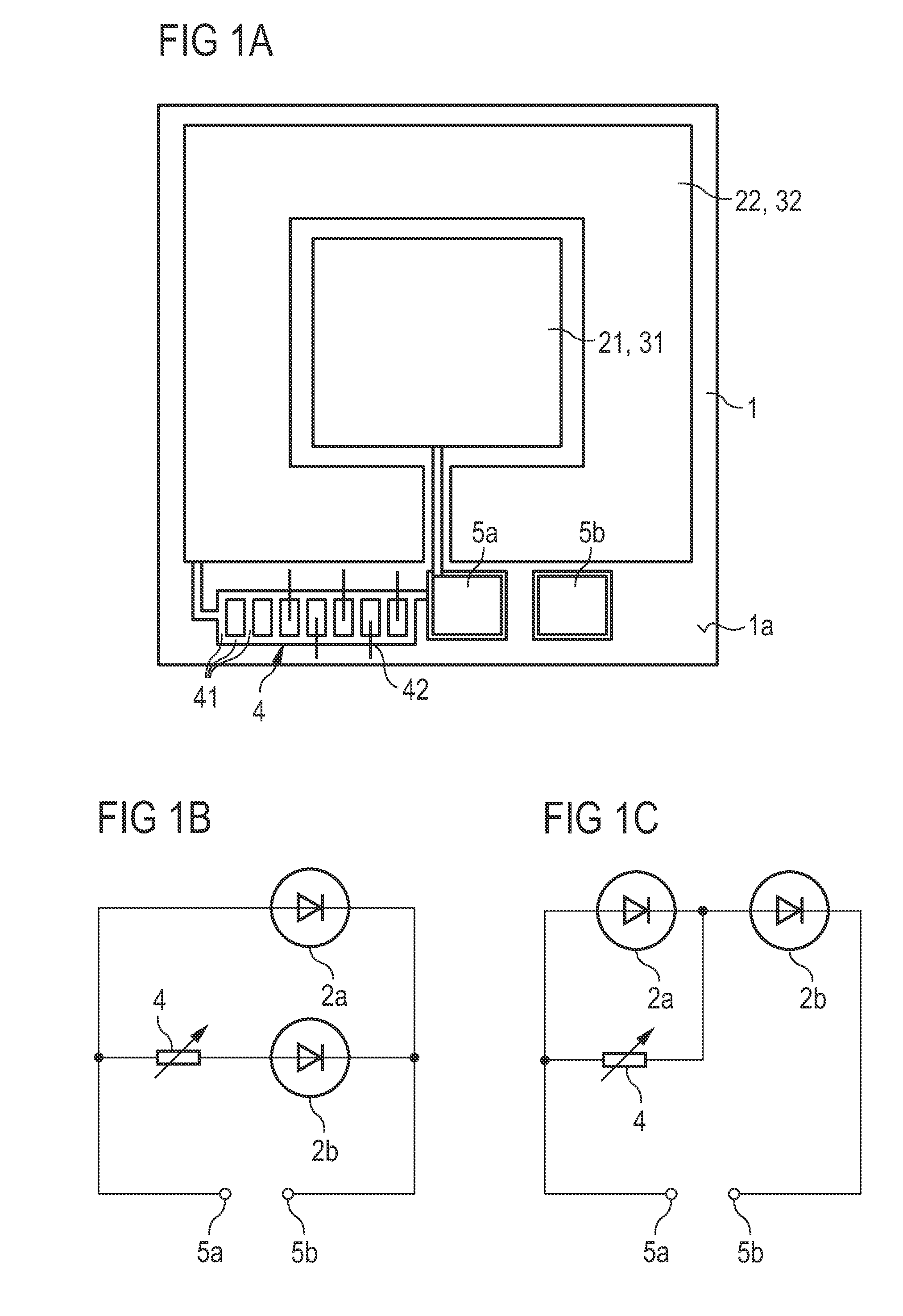
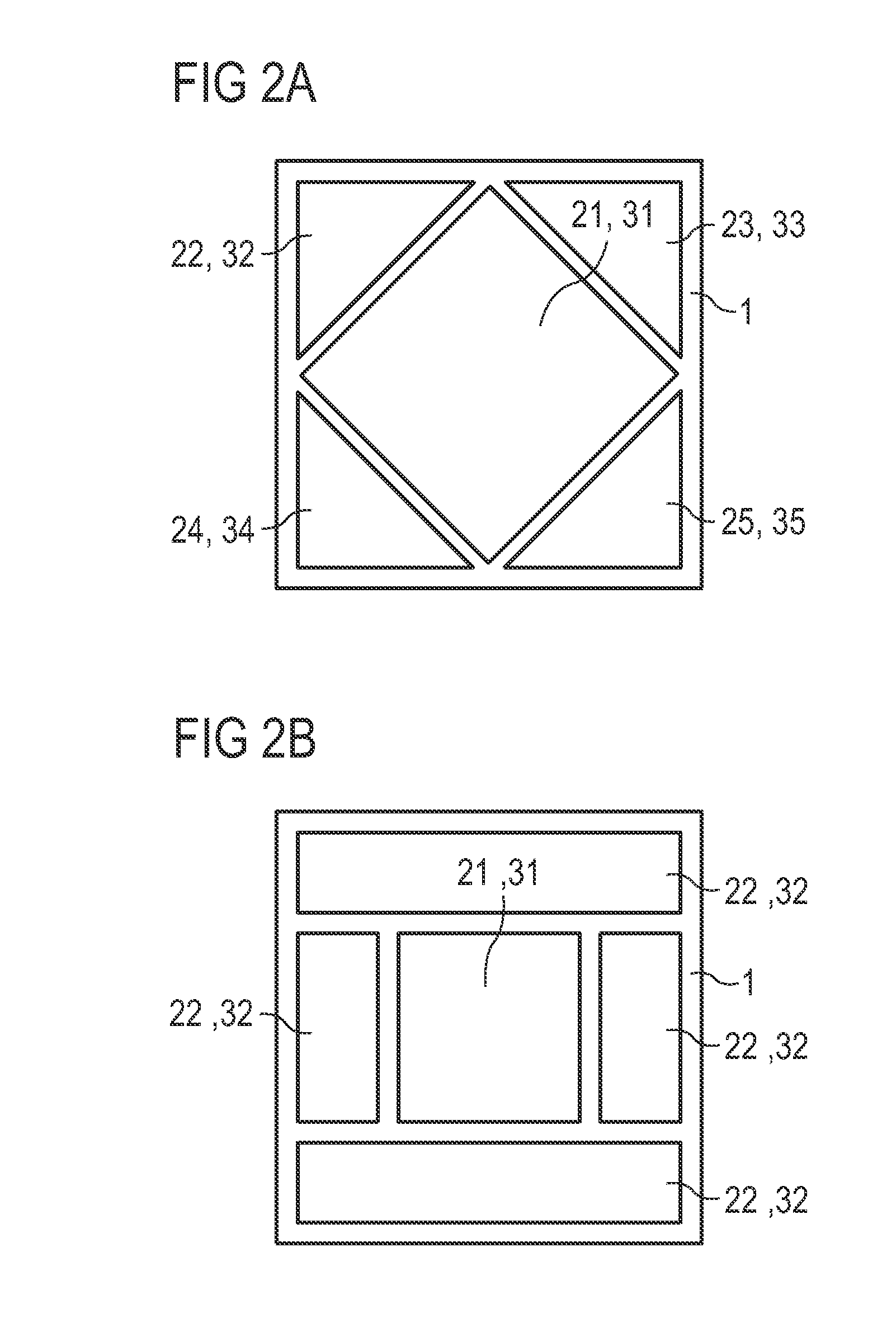
[0040]FIG. 1A shows a radiation-emitting semiconductor component described here in a schematic plan view.

[0041]The radiation-emitting semiconductor component comprises a light-emitting diode chip 1. In this exemplary embodiment, the light-emitting diode chip 1 has two emission areas 21, 22. The first emission area 21 is arranged centrally in a first main area 1a at the top side of the light-emitting diode chip 1. The first emission area 21 is enclosed in a lateral direction at least in places by the second emission area 22.

[0042]A conversion element 31, 32 is disposed downstream of each emission area, wherein the two conversion elements differ from one another. By way of example, the conversion elements are formed with different thicknesses. During the operation of the light-emitting diode chip 1, mixed light can be emitted from the emission areas 21, 22 at the same times, the mixed light being composed of the respective primary radiation and the respective secondary radiation.

[0043...


PUM


Abstract

A radiation-emitting semiconductor component includes a light-emitting diode chip with at least two emission regions that can be operated independently of each other and at least two differently designed conversion elements. During operation of the light-emitting diode chips each of the emission regions is provided for generating electromagnetic primary radiation. Each emission region has an emission surface by which at least part of the primary radiation is decoupled from the light-emitting diode chip. The conversion elements are provided for absorbing at least part of the primary radiation and for re-emitting secondary radiation. The differently designed conversion elements are disposed downstream of different emission surfaces. An electric resistance element is connected in series or parallel to at least one of the emission regions.

Description

[0001]This patent application is a national phase filing under section 371 of PCT / EP2010 / 061446, filed Aug. 5, 2010, which claims the priority of German patent application 10 2009 037 186.9, filed Aug. 12, 2009, each of which is incorporated herein by reference in its entirety.TECHNICAL FIELD[0002]A radiation-emitting semiconductor component is specified.[0003]U.S. Patent publication 2007 / 0252512 A1 describes a radiation-emitting semiconductor component.BACKGROUND[0004]In order to generate mixed-colored, in particular white, light with light-emitting diode chips, it is possible to use conversion elements in the beam path of the primary radiation emitted by the light-emitting diode chip, in order to convert part of the short-wave primary radiation into longer-wave secondary radiation.[0005]The intensity ratio of primary radiation to secondary radiation determines the emission color of the emitted light. In practice, firstly the wavelengths of the primary radiation from different ligh...

Claims


Application Information

Patent Timeline
IPC IPC(8): H01L33/50
CPCH01L27/153H01L33/08H01L33/382H01L33/50H01L33/62H01L33/20H01L2924/3011H01L33/32H01L2224/49107H01L2924/00
Inventor VON MALM, NORWINWIRTH, RALPH
Owner OSRAM OPTO SEMICONDUCTORS GMBH
Why Eureka
Try Eureka