
Nanostructuring process for ingot surface, wafer manufacturing method, and wafer using the same

Active Publication Date: 2012-08-02
SINO AMERICAN SILICON PROD
View PDF8 Cites 8 Cited by
  • Summary
  • Abstract
  • Description
  • Claims
  • Application Information

AI Technical Summary

Benefits of technology

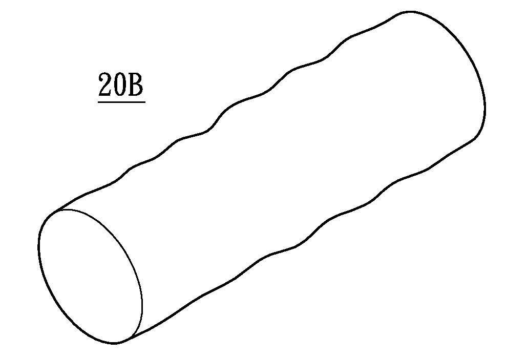
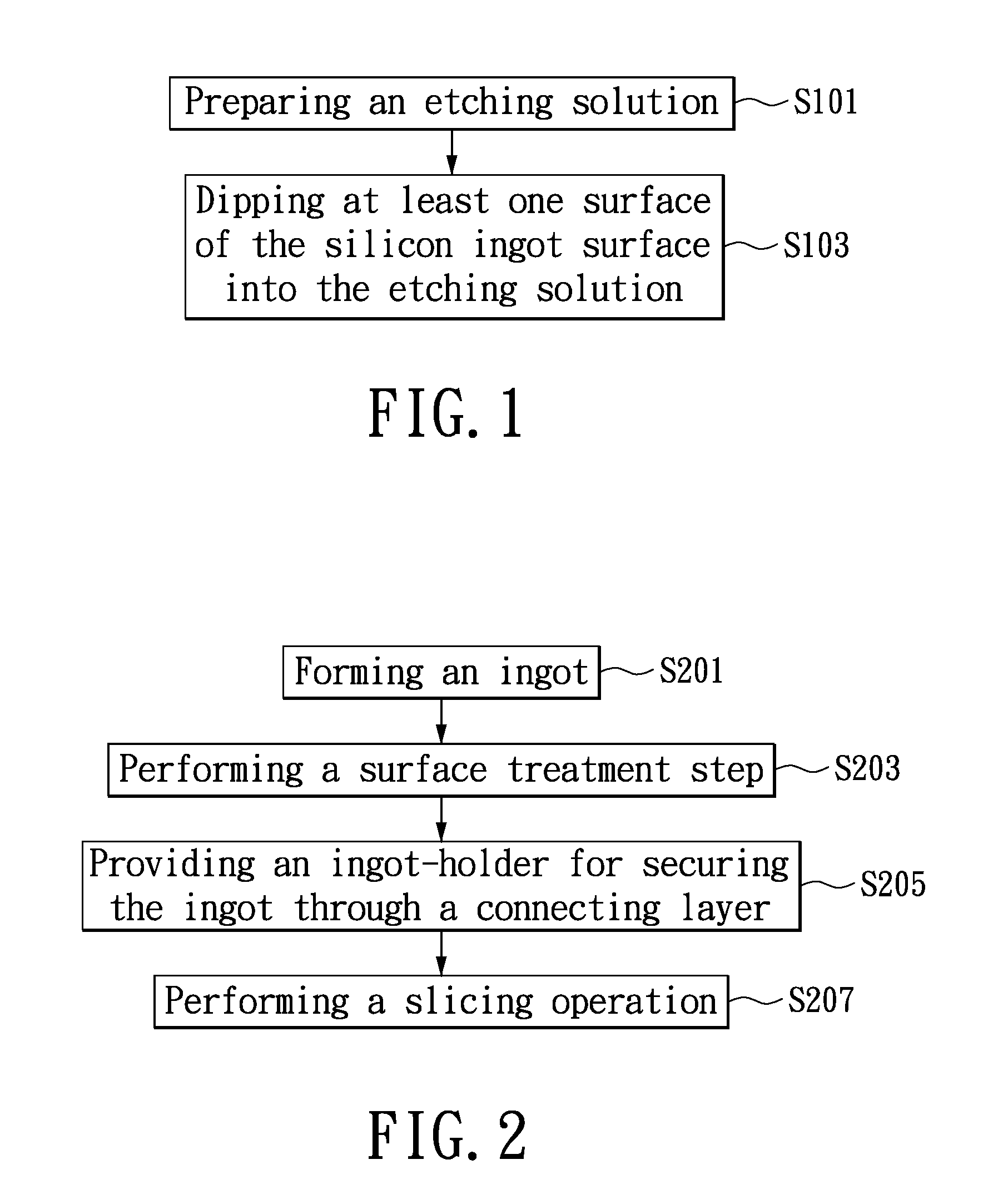
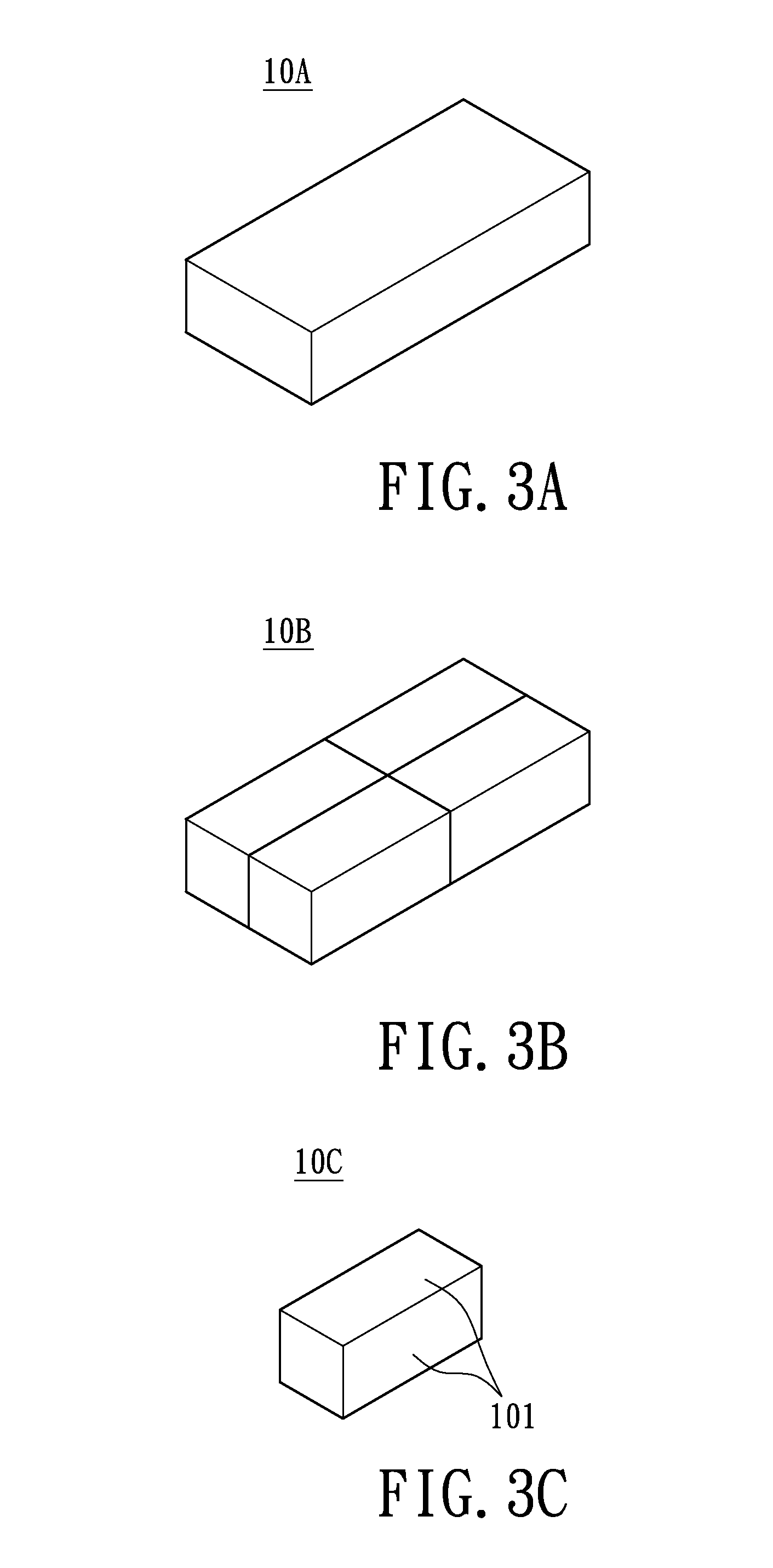
[0008]An object of the instant disclosure is to provide a nanostructuring process for an ingot surface and a wafer manufacturing method using the same. The ingot surface is treated in forming nanostructures thereon prior to the slicing process. The nanostructure layer is capable of increasing the surface strength of the ingot to reduce the occurrence of cracking and breaking.
[0013]Based on the above, the instant disclosure utilizes a surface treatment method to change at least one side surface of the ingot by forming the nanostructure layer on the side surface, without changing the original surface properties of the ingot. This nanostructure layer is capable of improving the mechanical strength of the ingot to reduce the chipping issue during the slicing process.

Problems solved by technology

However, for an ingot that is more brittle, the machining process may lead to excessive scraps.
Namely, the cutting tools can cause surface cracks for the ingot and form microscopic cracks around the periphery of the wafers.
These wafers are more likely to break or crack during subsequent refining processes, resulting lower yield rate.
When these external forces exceed the maximum strength of the wafer or are over-concentrated on the wafer, the wafer may crack or break resulting in a poor yield rate.

Method used


Image

  • Nanostructuring process for ingot surface, wafer manufacturing method, and wafer using the same
  • Nanostructuring process for ingot surface, wafer manufacturing method, and wafer using the same
  • Nanostructuring process for ingot surface, wafer manufacturing method, and wafer using the same

Examples


Embodiment Construction

[0025]The instant disclosure provides a nanostructuring process for an ingot surface and a wafer manufacturing method using the same. Before the ingot is being sliced, the nanostructuring process involves treating at least one surface of the ingot in forming a nanostructure layer thereon. This nanostructure layer is capable of dispersing external stress to reduce the chipping ratio during the slicing operation, thereby increasing the yield rate and quality of the wafers.

[0026]The nanostructuring process utilizes the wet etching technique to restructure the ingot surface. The formed nanostructure may have a needle-like shape or be cylindrical shaped. For the instant embodiment, the formed nanostructure has a grass-like shape and may be referred to as the silicon grass structure, or as black silicon. The term “black silicon” derives from the fact after the ingot has undergone surface treatment, the ingot will appear substantially black in color. The black silicon absorbs nearly all th...


PUM


Abstract

The instant disclosure relates to a nanostructuring process for an ingot surface prior to the slicing operation. A surface treatment step is performed for at least one surface of the ingot in forming a nanostructure layer thereon. The nanostructure layer is capable of enhancing the mechanical strength of the ingot surface to reduce the chipping ratio of the wafer during slicing.

Description

BACKGROUND OF THE INVENTION[0001]1. Field of the Invention[0002]The instant disclosure relates to a nanostructuring process for surface treatment; in particular, to a nanostructuring process applicable to an ingot surface, a wafer manufacturing method, and a wafer using the same.[0003]2. Description of Related Art[0004]Information products and appliances utilized in daily life such as cell phones, computer motherboards, micro-processors, memory devices, digital cameras, personal digital assistants (PDA), etc., use integrated circuits (IC). Generally speaking, integrated circuits refer to the use of wafers undergone different semiconductor fabrication processes in creating various individual circuit elements.[0005]The semiconductor fabrication process involves crystallization (ingot forming), surface grinding, slicing, polishing, and cleaning. When the ingot is sliced to form wafers, the slicing process determines how many wafers and chips that can be made in subsequent processes. Th...

Claims


Application Information

Patent Timeline
IPC IPC(8): H01L21/306H01L29/30B82Y30/00B82Y40/00
CPCC30B29/06C30B33/10C30B33/00Y10T428/24777H01L29/16
Inventor CHYAN, JIUNN-YIHLI, JIAN-JHIHYANG, KUN-LINHSU, WEN-CHING
Owner SINO AMERICAN SILICON PROD
Learn More