Power supply circuit, control method for controlling power supply circuit, and electronic device incorporating power supply circuit
- Summary
- Abstract
- Description
- Claims
- Application Information
AI Technical Summary
Benefits of technology
Problems solved by technology
Method used
Image

Examples
first embodiment
Variation of First Embodiment
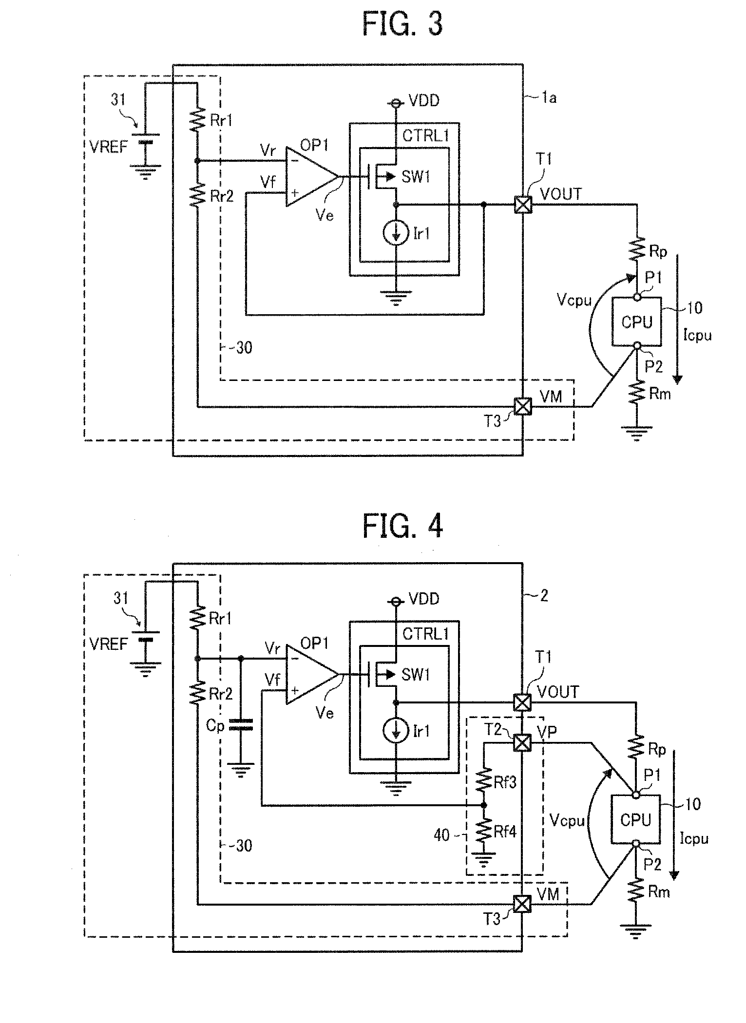
[0035]FIG. 3 is a circuit diagram illustrating a configuration of a power supply circuit 1a according to a variation of the first embodiment. In the power supply circuit 1a of the variation of the first embodiment, the load voltage detection terminal T2 and the resistors Rf3 and Rf4 are eliminated from the configuration of the power supply circuit 1 shown in FIG. 2, and the output voltage VOUT at the output terminal T1 of the power supply circuit 1a functions directly as the load detection voltage Vf. Thus, the parasitic resistor Rp is not taken into account but the parasitic resistor Rm is taken into account. Therefore, similar to the power supply circuit 1 shown in FIG. 2, in the power supply circuit 1a, the voltage error caused by the parasitic voltage drop can be minimized without increasing either the consumption of current or the chip size, enabling supply of a highly accurate and stable voltage to the load circuit 10 such as CPU.
Second Embodiment
[...
second embodiment
Variation of Second Embodiment
[0037]FIG. 5 is a circuit diagram illustrating a configuration of a power supply circuit 2a according to a variation of the second embodiment. Comparing to the power supply circuit 2 shown in FIG. 4, the load voltage detection terminal T2 and the resistors Rf3 and Rf4 are eliminated in the power supply circuit 2a, and the output voltage VOUT at the output terminal T1 of the power supply circuit 2a functions directly as the load detection voltage Vf. Thus, the parasitic resistor Rp is not taken into account, but the parasitic resistor Rm is taken into account. Therefore, similarly to the power supply circuit 2 shown in FIG. 4, in the power supply circuit 2a, the voltage error caused by the parasitic voltage drop can be minimized without increasing either the consumption of current or the chip size, enabling supply of a highly accurate and stable voltage to the load circuit 10 such as CPU.
third embodiment
[0038]FIG. 6 is a circuit diagram illustrating a configuration of a power supply circuit 3 according to a third embodiment. A distinctive feature of the present embodiment is that the power supply circuit 3 is formed by a switching regulator instead of the linear regulator. A control circuit CTRL1a of the switching regulator 3 includes a clock generator 11, a SR-type flip-flop circuit 12, an inverter 13, a CMOS (Complementary Metal Oxide Semiconductor) circuit constituted by switching transistors SW1 and SW2, a current detector 14, a current-voltage converter (hereinafter “I / V converter”) 15, and an error amplifier OP2. In addition, a low-pass filer 20 to remove high-frequency and smooth the voltage, constituted by an inductor L1 and a capacitor C1, is provided between the output terminal T1 of the power supply circuit 3 and the parasitic resistor Rp.
[0039]Operation of the switching regulator 3 is described below. In the control circuit CTRL1a shown in FIG. 6, the error amplifier OP...
PUM
 Abstract
Description
Claims
Application Information
 - R&D Engineer
- R&D Manager
- IP Professional
- Industry Leading Data Capabilities
- Powerful AI technology
- Patent DNA Extraction
Browse by: Latest US Patents, China's latest patents, Technical Efficacy Thesaurus, Application Domain, Technology Topic.
© 2024 PatSnap. All rights reserved.Legal|Privacy policy|Modern Slavery Act Transparency Statement|Sitemap