

High Bandwidth Passive Switching Current Sensor
a passive switching current and high bandwidth technology, applied in the field of integrated circuits, can solve the problems of significant design challenges, difficult high frequency measurement, and design or under design of power delivery networks, and achieve the effects of accurate power and load analysis, accurate sensing of switching current activity, and high sensitiveness
- Summary
- Abstract
- Description
- Claims
- Application Information
AI Technical Summary
Benefits of technology
Problems solved by technology
Method used
Image

Examples
Embodiment Construction
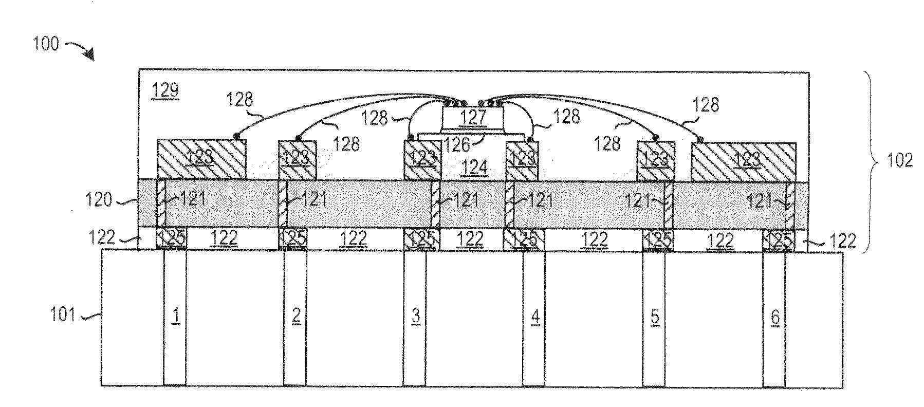
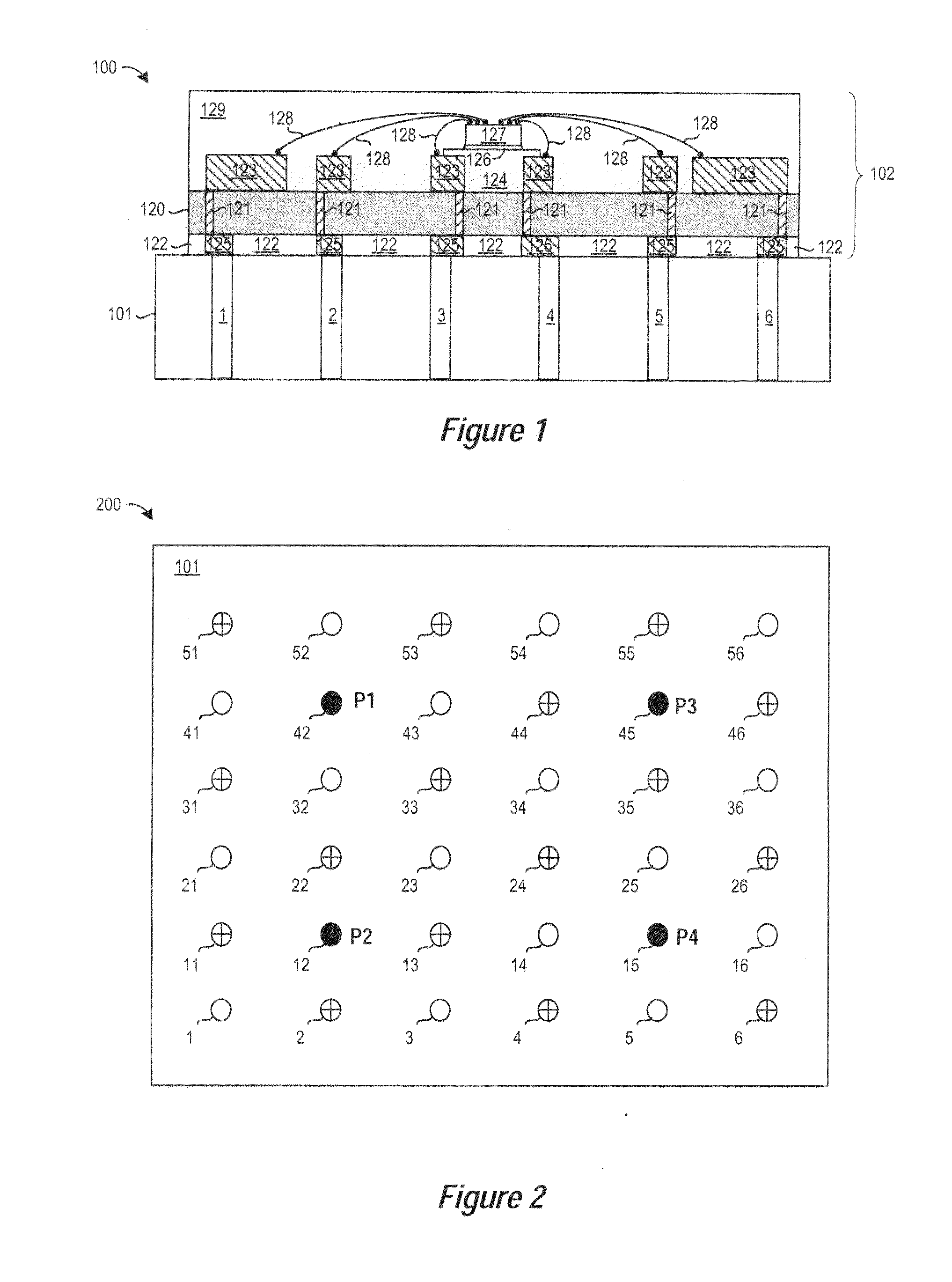
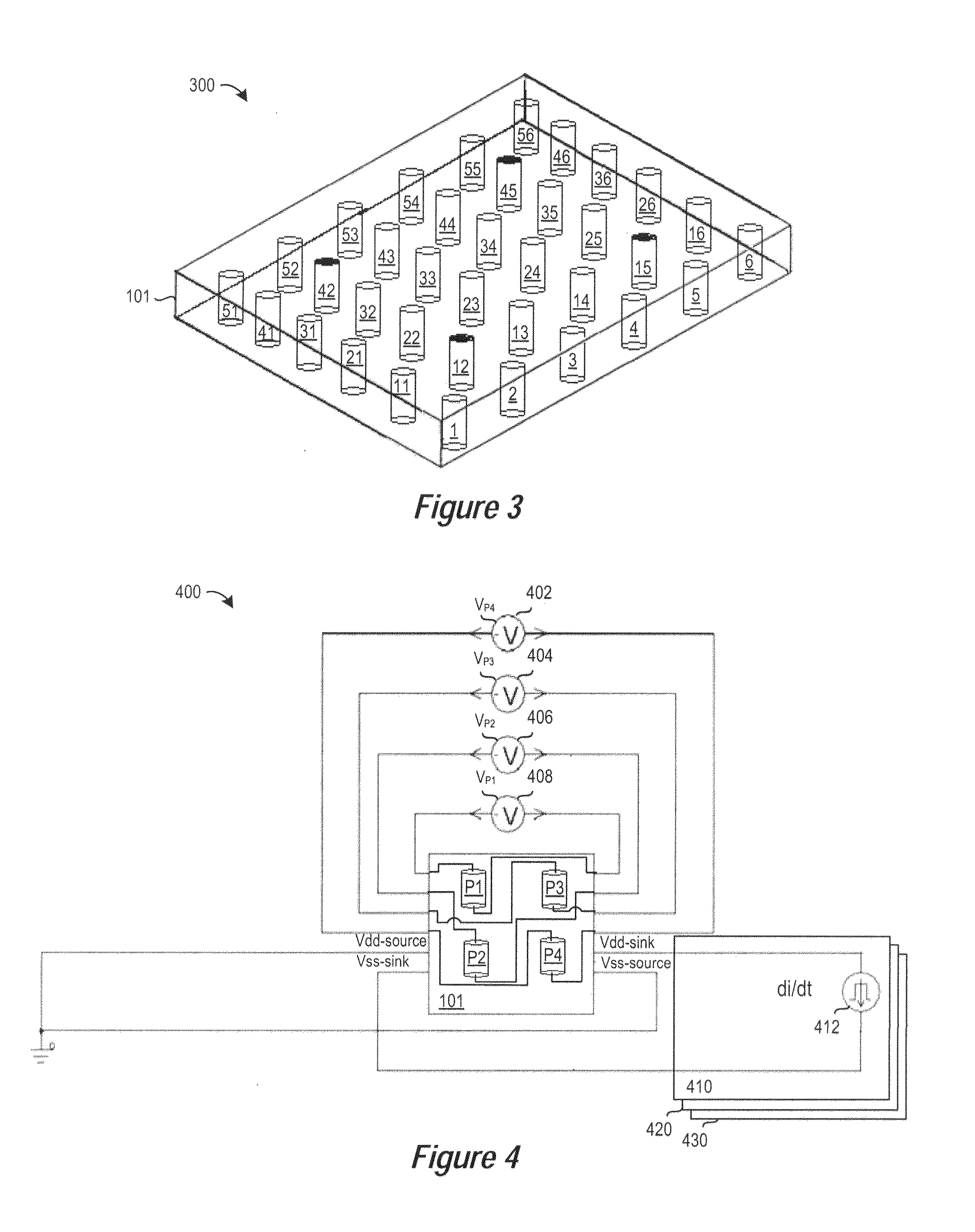
[0006]Broadly speaking, embodiments of the present invention provide a system, method and dynamic current sensor apparatus for sensing fast current switching events by forming one or more passive current sensing structures within sensing proximity to one or more power and / or ground conductors. In selected embodiments, the power and / or ground conductors may be formed in the printed circuit board substrate as an array of plated through holes (PTH) that surround the power and / or ground conductors that are also formed in the printed circuit board substrate or electronic packaging. Thus positioned within sensing proximity to the power and / or ground conductors, the passive current sensing structures are able to sense current switching activity in the power and / or ground conductors by converting dynamic changes in the power supply current into a measurable voltage signal. In addition to accurately sensing switching current activity with available package or PCB manufacturing technology, th...
PUM
 Abstract
Description
Claims
Application Information