Light-emitting device and lighting device

a technology of light-emitting devices and lighting devices, which is applied in the direction of thermoelectric devices, electroluminescent light sources, electric lighting sources, etc., can solve the problems of patterning defect and increase manufacturing costs, and achieve the reduction of the light-emitting area in the light-emitting region, the effect of increasing the resistance of lead wiring and increasing the width of the lead wir

Inactive Publication Date: 2012-08-16
SEMICON ENERGY LAB CO LTD
View PDF1 Cites 24 Cited by
  • Summary
  • Abstract
  • Description
  • Claims
  • Application Information

AI Technical Summary

Benefits of technology

[0007]In the case where a lighting device is formed using a plurality of light-emitting elements, the plurality of light-emitting elements are connected to one another by a lead wiring. Even when a low resistance metal is used, the lead wiring is long and the resistance thereof is increased; therefore, the width of the lead wiring needs to be larger than that of a wiring used in a light-emitting region. When the width of the lead wiring is increased, the light-emitting area in the light-emitting region is reduced or the aperture ratio is decreased.

Problems solved by technology

Patterning with a metal mask has a problem of causing defects in patterning caused by bending or warping of a metal mask.
Thus, the yield is decreased, which leads to an increase of manufacturing cost.

Method used


Image

  • Light-emitting device and lighting device
  • Light-emitting device and lighting device
  • Light-emitting device and lighting device

Examples


embodiment 1

[0028]In this embodiment, a light-emitting device according to one embodiment of the present invention is described with reference to FIG. 1 and FIGS. 2A and 2B.

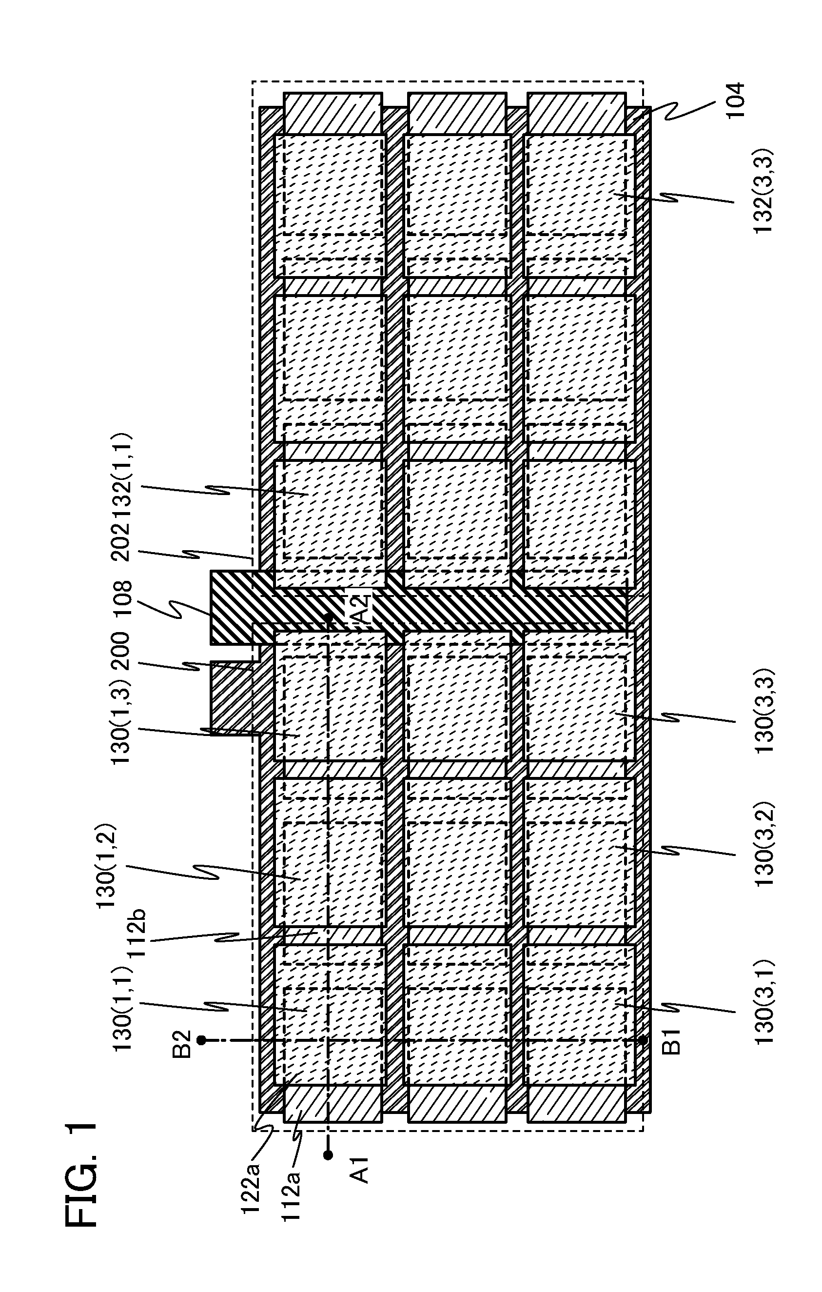
[0029]FIG. 1 is an enlarged plan view of part of the light-emitting device according to one embodiment of the present invention. Note that in FIG. 1, only wirings and electrodes are illustrated and an insulating film and the like are omitted.

[0030]The light-emitting device according to one embodiment of the present invention includes a light-emitting element unit 200 and a light-emitting element unit 202. The light-emitting element unit 200 and the light-emitting element unit 202 are connected to a converter (not illustrated) through a first wiring 104 and a second wiring 108. The converter is provided to convert high voltage input from an external commercial power supply (e.g., approximately 100 V to 240 V) to voltage at which a light-emitting element is driven (e.g., approximately 3 V to several tens of volts). Different v...

embodiment 2

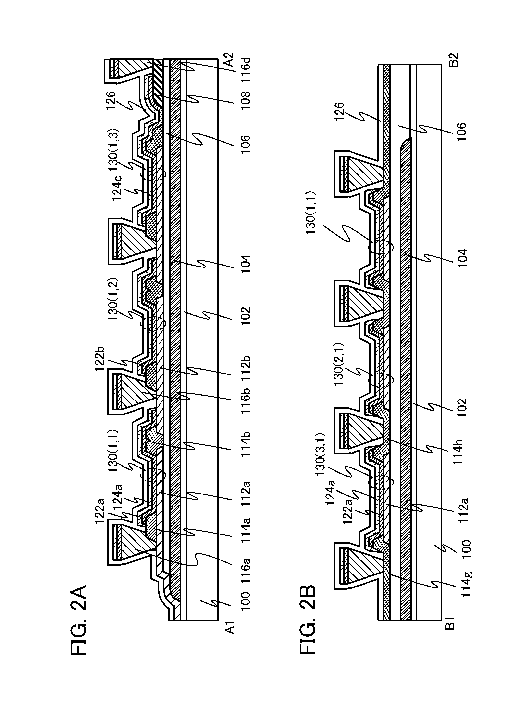
[0068]In this embodiment, a method for manufacturing a lighting device according to one embodiment of the present invention is described with reference to FIGS. 3A to 3C, FIGS. 4A and 4B, and FIGS. 5A to 5C. Note that the manufacturing method illustrated in FIGS. 3A to 3C, FIGS. 4A and 4B, and FIGS. 5A to 5C is steps in the cross section taken along line A1-A2 in FIG. 1.

[0069]First, the insulating film 102 is formed as a base film over the substrate 100. For the substrate 100 and the insulating film 102, description in Embodiment 1 can be referred to. In this embodiment, a stainless steel substrate is used as the substrate 100. As the insulating film 102, a silicon oxynitride film having a thickness of 100 nm is formed by a CVD method.

[0070]Next, the first wiring 104 is formed over the insulating film 102. In this embodiment, as the first wiring 104, a film containing silver with a thickness of 20 μm is formed using a silver paste by a printing method (see FIG. 3A).

[0071]Next, the i...

embodiment 3

[0087]In this embodiment, a lighting device in which the light-emitting device described in the above embodiment is described with reference to FIG. 6.

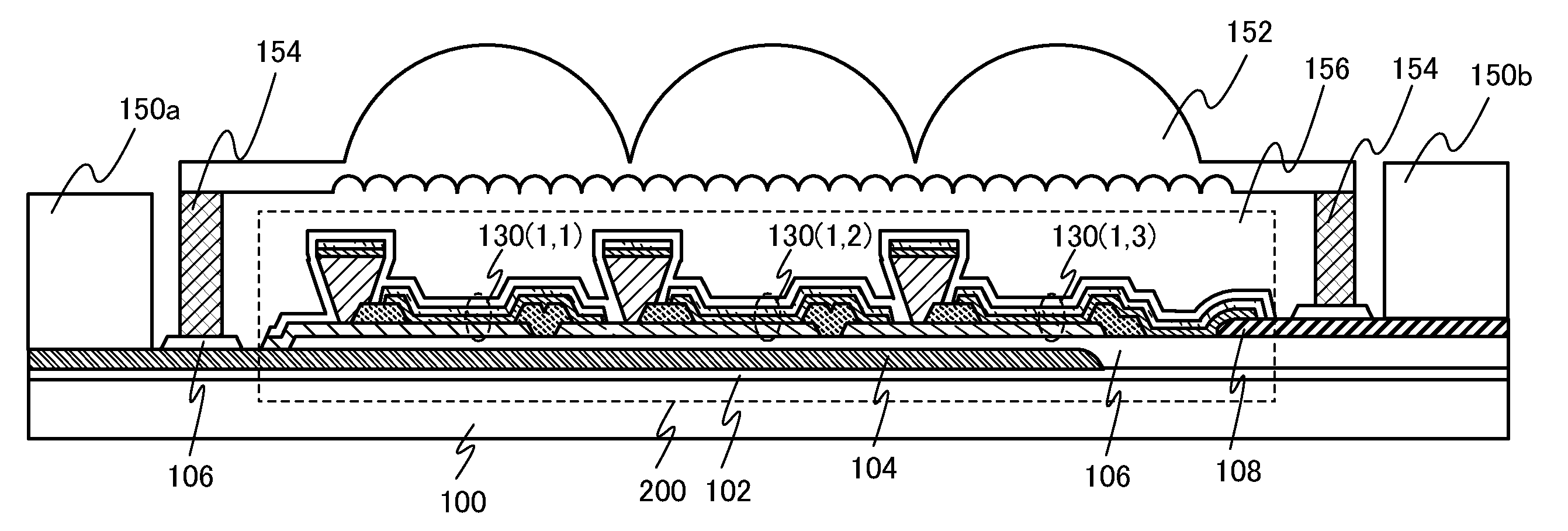
[0088]FIG. 6 is a cross-sectional view of a lighting device according to one embodiment of the present invention. As a light source of the lighting device, a light-emitting device including the light-emitting element unit 200 can be used.

[0089]The first wiring 104 is provided over the substrate 100 with the insulating film 102 provided therebetween, and the second wiring 108 and the light-emitting element unit 200 are provided over the first wiring 104 with the insulating film 106 provided therebetween. The substrate 100 and an optical element 152 are bonded to each other with a sealant 154. A space surrounded by the substrate 100, the optical element 152, and the sealant 154 is filled with a high refractive resin 156. In the substrate 100, converters 150a and 150b are provided on the outer side of the region surrounded by the sealant...


PUM


Abstract

To provide a light-emitting device including the plurality of light-emitting elements having a structure in which a light-emitting area is large and defects in patterning of light-emitting elements are suppressed. To provide a lighting device including the light-emitting device. The light-emitting device includes a first wiring provided over a substrate having an insulating surface, an insulating film provided over the first wiring, a second wiring provided over the insulating film, and a light-emitting element unit including a plurality of light-emitting elements provided over the first wiring with the insulating film provided therebetween. The plurality of light-emitting elements each include a first electrode layer having a light-blocking property, a layer containing an organic compound in contact with the first electrode layer, and a second electrode layer having a light-transmitting property in contact with the layer containing an organic compound. The layers containing an organic compound are separated by a separation layer.

Description

BACKGROUND OF THE INVENTION[0001]1. Field of the Invention[0002]The present invention relates to a light-emitting element unit including a plurality of light-emitting elements utilizing organic electroluminescence (EL) (hereinafter, also referred to as an organic EL element). The present invention also relates to a light-emitting device and a lighting device each including the light-emitting element unit.[0003]2. Description of the Related Art[0004]An organic EL element has a structure in which a layer containing a light-emitting organic compound is interposed between a pair of electrodes. By applying voltage to this element, light emission from the light-emitting organic compound can be obtained. In recent years, the organic EL element has been expected to be applied to a light source of a lighting device.[0005]In Patent Document 1, a lighting device having a structure in which a plurality of organic EL elements are connected in series is disclosed. With the use of a plurality of o...

Claims


Application Information

Patent Timeline
Patent Type & Authority Applications(United States)
IPC IPC(8): H01L27/15H01L33/36H05B44/00
CPCH01L27/3202H01L27/3246H01L27/3204H10K59/84H10K59/86H10K59/122
Inventor YAMAZAKI, SHUNPEIONO, KOJITANADA, YOSHIFUMI
Owner SEMICON ENERGY LAB CO LTD
Why Eureka
Try Eureka