Light-emitting diode device

a technology of light-emitting diodes and led chips, which is applied in the direction of semiconductor devices, basic electric elements, electrical equipment, etc., can solve the problems of led chip electrical reliability and light output by various portions, and achieve the effect of improving electrical reliability and phosphor coating

Inactive Publication Date: 2012-08-16
SEMILEDS OPTOELECTRONICS CO LTD +1
View PDF7 Cites 26 Cited by
  • Summary
  • Abstract
  • Description
  • Claims
  • Application Information

AI Technical Summary

Benefits of technology

[0009]Light-emitting diode (LED) devices having light-emitting diode (LED) chips with an improved phosphor coating formed thereover and improved electrical reliability thereof are provided.

Problems solved by technology

This is undesired since shorts may be happen to the LED chip during the selective electrophoretic phosphor deposition process, thereby ruining electrical reliability of the LED chip.
In addition, in U.S. Pat. No. 6,576,488, the phosphor particles are deposited over the LED chip at a relative slow deposition rate during the selective electrophoretic phosphor deposition process, wherein some of the charged phosphor particles coated over the LED chip may crack and peel off from the LED chip, thereby causing light to be output by various portions of the LED chip.

Method used


Image

  • Light-emitting diode device
  • Light-emitting diode device
  • Light-emitting diode device

Examples


Embodiment Construction

[0016]The following description is of the best-contemplated mode of carrying out the invention. This description is made for the purpose of illustrating the general principles of the invention and should not be taken in a limiting sense. The scope of the invention is best determined by reference to the appended claims.

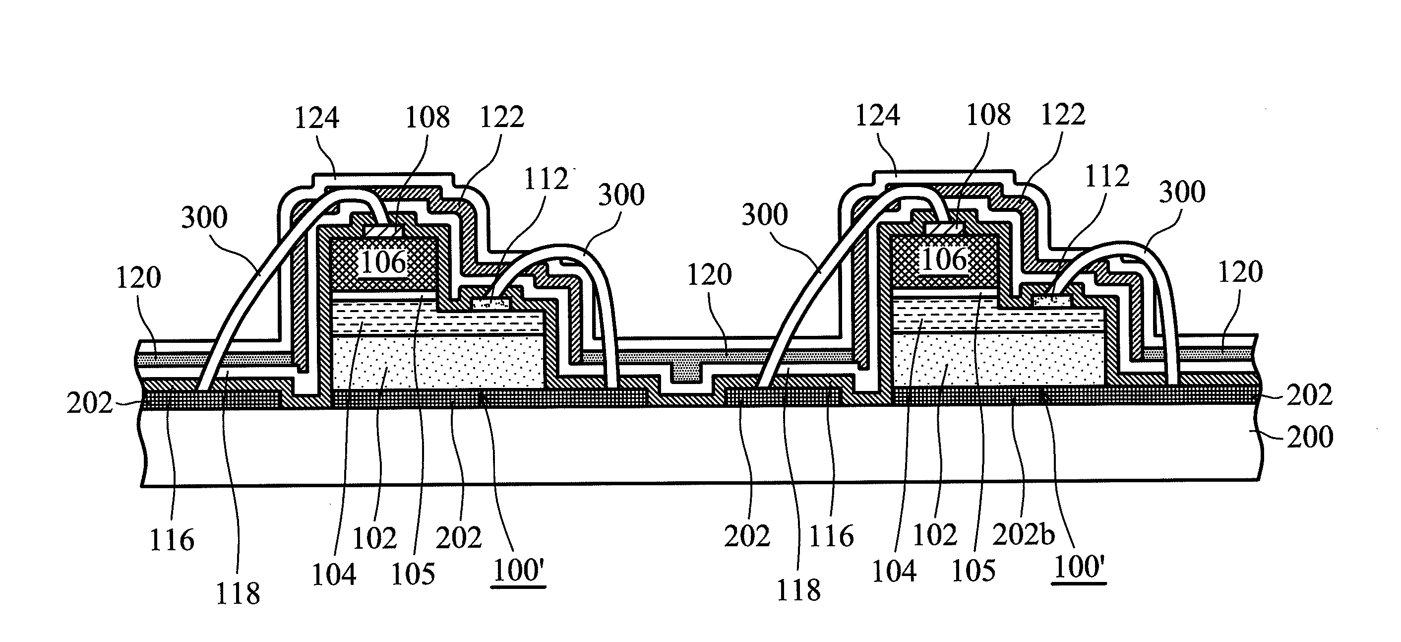
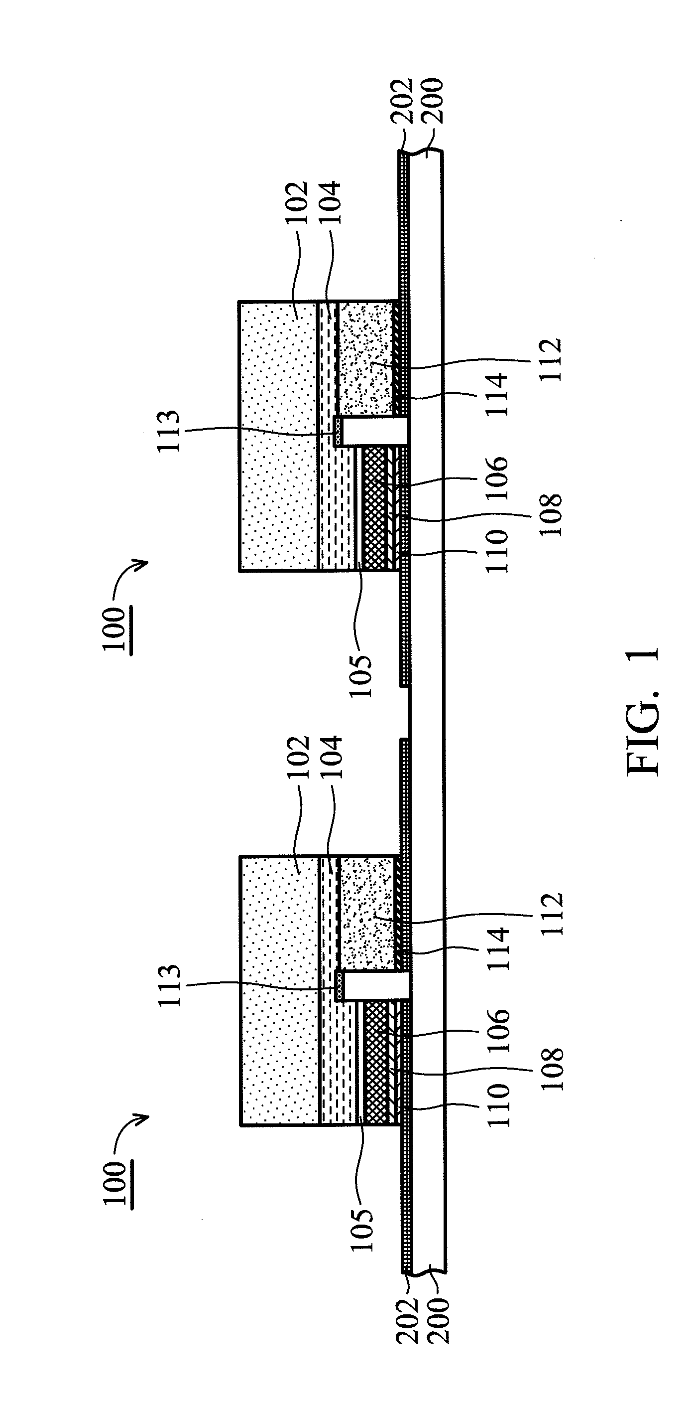
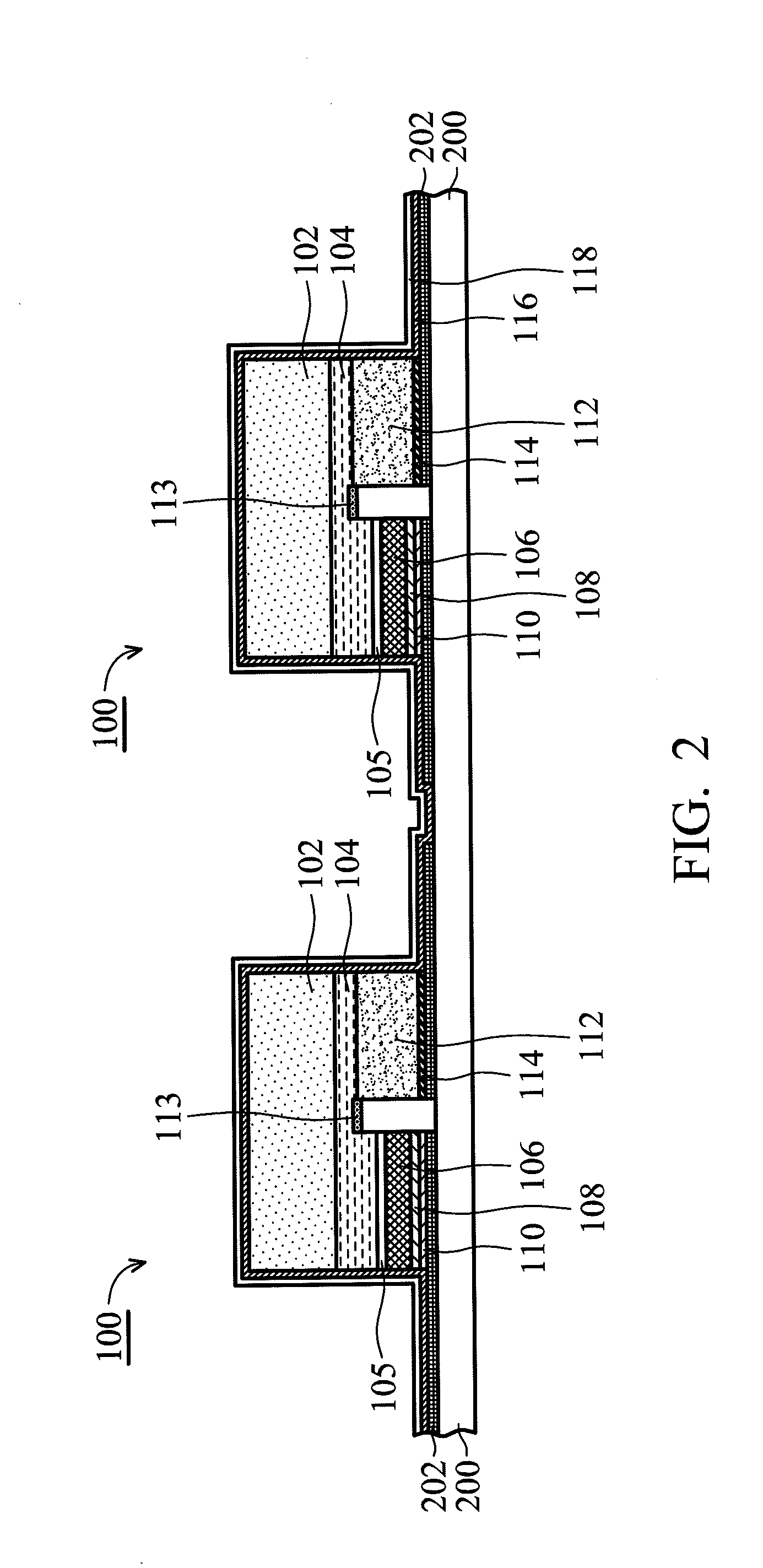
[0017]As used herein, “LED chip” refers to a stack of semiconductor layers, including an active region which emits light when biased to produce an electrical current flow through the device, and contacts attached to the stack. If a substrate on which the semiconductor layers are grown is present, “LED chip” includes the substrate. “Phosphor” refers to any luminescent materials which absorb light of one wavelength and emits light of a different wavelength. “Submount,” used herein, refers to a secondary support substrate other than the substrate on which the epitaxial layers of an LED chip are grown.

[0018]FIGS. 1-5, and 7 are cross sections showing an exemplary method fo...


PUM


Abstract

A light-emitting diode device is provided, including a submount, a light-emitting diode (LED) chip mounted on the submount, a first transparent insulating layer formed on the submount and the LED chip, a transparent conductive layer formed on the first transparent insulating layer, a phosphor layer formed on the first transparent conductive layer covering the LED chip, and a transparent passivation layer formed on the phosphor layer and over the transparent conductive layer.

Description

BACKGROUND OF THE INVENTION[0001]1. Field of the Invention[0002]The invention relates to light emitting devices, and more particularly to light-emitting diode (LED) devices having a light-emitting diode (LED) chip with an improved phosphor coating thereover and improved electrical reliability thereof.[0003]2. Description of the Related Art[0004]Light-emitting diode (LED) devices are solid-state light sources with multiple-advantages. They are capable of reliably providing light with high brightness and thus are applied in displays, traffic lights and indicators. LED devices typically include an LED die electrically bonded on a support substrate and the LED die may have an n-contact formed on one side and a p-contact formed on the opposite side therein or have both contacts formed on the same side therein.[0005]To improve light output efficiency of an LED device, uniform light output performances of the LED device needs to be improved. U.S. Pat. No. 6,576,488, issued to Collins, III ...

Claims


Application Information

Patent Timeline
Patent Type & Authority Applications(United States)
IPC IPC(8): H01L33/44
CPCH01L33/42H01L2933/0041H01L33/507H01L33/44H01L2224/16225H01L2224/48091H01L2224/48227H01L2224/49107H01L2224/8592H01L2924/00014
Inventor LIN, TZU-HANLIN, IZY-YINGLIN, MING-NAN
Owner SEMILEDS OPTOELECTRONICS CO LTD
Why Eureka
Try Eureka