

3-d structured non-volatile memory device and method of manufacturing the same
a non-volatile memory and structured technology, applied in the field of non-volatile memory devices, can solve problems such as the characteristics of memory devices deteriorating
- Summary
- Abstract
- Description
- Claims
- Application Information
AI Technical Summary
Benefits of technology
Problems solved by technology
Method used
Image

Examples
first embodiment
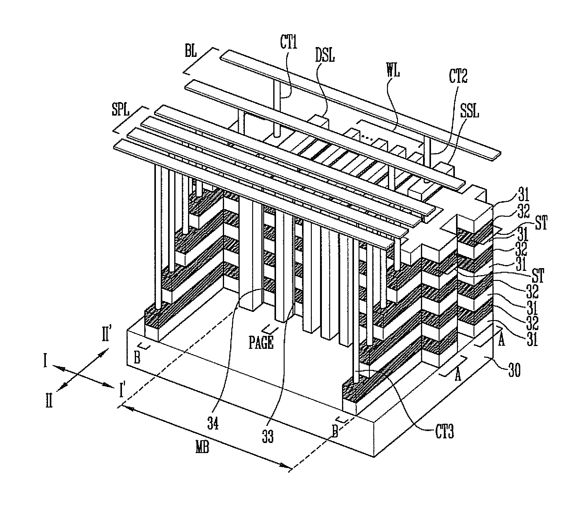
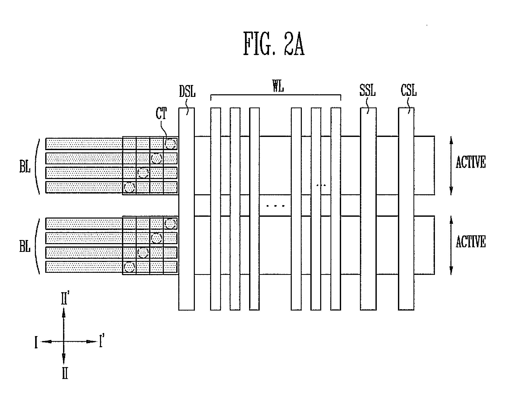
[0024]FIG. 2A is a layout diagram of a 3-D structured non-volatile memory device according to this disclosure.
[0025]As shown in FIG. 2A, the 3-D structured non-volatile memory device according to the first embodiment of this disclosure includes a plurality of active regions ACTIVE extended in a first direction I-I′. A plurality of channel layers are stacked in each of the active regions ACTIVE.
[0026]The 3-D structured non-volatile memory device further includes a drain select line DSL, a plurality of word lines WL, a source select line SSL, and a common source line CSL which are each arranged in a second direction II-II′ crossing the first direction I-I′.
[0027]The 3-D structured non-volatile memory device further includes a plurality of bit lines BL coupled to respective channel layers stacked over in each of the active regions ACTIVE and each extended in the first direction I-I′. The bit lines BL are coupled to the respective channel layers through the respective contact plugs CT.
[...
second embodiment
[0038]FIG. 3A is a layout diagram of a 3-D structured non-volatile memory device according to this disclosure.
[0039]As shown in FIG. 3A, the 3-D structured non-volatile memory device according to the second embodiment includes a plurality of active regions ACTIVE extended in a first direction I-I′. A plurality of channel layers is stacked in each of the active regions ACTIVE.
[0040]The 3-D structured non-volatile memory device further includes a drain select line DSL, a plurality of word lines WL, a plurality of source select lines SSL, and a source line SL which are arranged in a second direction II-II′ crossing the first direction I-I′. Here, the source select line SSL is formed in each active region ACTIVE. The source line SL has a stack structure of plural source lines SL, and it is coupled the plurality of channel layers formed in the active regions ACTIVE.
[0041]Furthermore, one bit line BL is coupled to each active region ACTIVE. The bit line BL is extended in the first directi...
third embodiment
[0085]FIG. 5 is a perspective view of a 3-D structured non-volatile memory device according to this disclosure.
[0086]The memory device of the third embodiment has substantially the same structure as the memory device of the second embodiment except that the plurality of source lines 42D included in the source structures B is silicided.
[0087]The source lines 42D may be silicided by forming the source structures B by etching the source blocks C (refer to FIGS. 4A and 4G). In this case, the silicided source lines 42D may be formed by filling a metal layer in a gap region between the adjacent source structures B and making the metal layer and the source lines 42B react with each other through an annealing process. Here, some of the source lines 42B may be silicided.
[0088]The metal layer may be made of cobalt (Co), titanium (Ti), or nickel (Ni). The metal layer may react with the source lines 42B formed of a polysilicon layer, thus forming the source lines 42D including cobalt silicide, ...
PUM
 Abstract
Description
Claims
Application Information