Methods and systems for reducing polarization dependent loss

a technology of polarization dependent loss and reduction method, applied in the field of photonic integrated circuits, can solve the problems of high coupling loss, high cost, and difficult light coupling between optical elements such as optical fibers and optical waveguides, and achieve the effects of low polarization dependent loss, reduced or no polarization dependent loss, and reduced or avoided polarization dependent loss inherently induced by two-dimensional ( 2d ) grating couplers

Inactive Publication Date: 2012-08-16
UNIV GENT +1
View PDF8 Cites 29 Cited by
  • Summary
  • Abstract
  • Description
  • Claims
  • Application Information

AI Technical Summary

Benefits of technology

[0007]It is an object of the present invention to provide good photonic integrated circuits using two-dimensional grating couplers having low, reduced or no polarization dependent loss. It is

Problems solved by technology

However, coupling of light between an optical element such as for example an optical fiber and an optical waveguide, e.g. an optical waveguide on a silicon chip, is challenging because of the large mismatch in mode-size between the integrated nanophotonic waveguides (typically 0.1 μm2) and standard single mode fibers (typically 100 μm2

Method used


Image

  • Methods and systems for reducing polarization dependent loss
  • Methods and systems for reducing polarization dependent loss
  • Methods and systems for reducing polarization dependent loss

Examples


Embodiment Construction

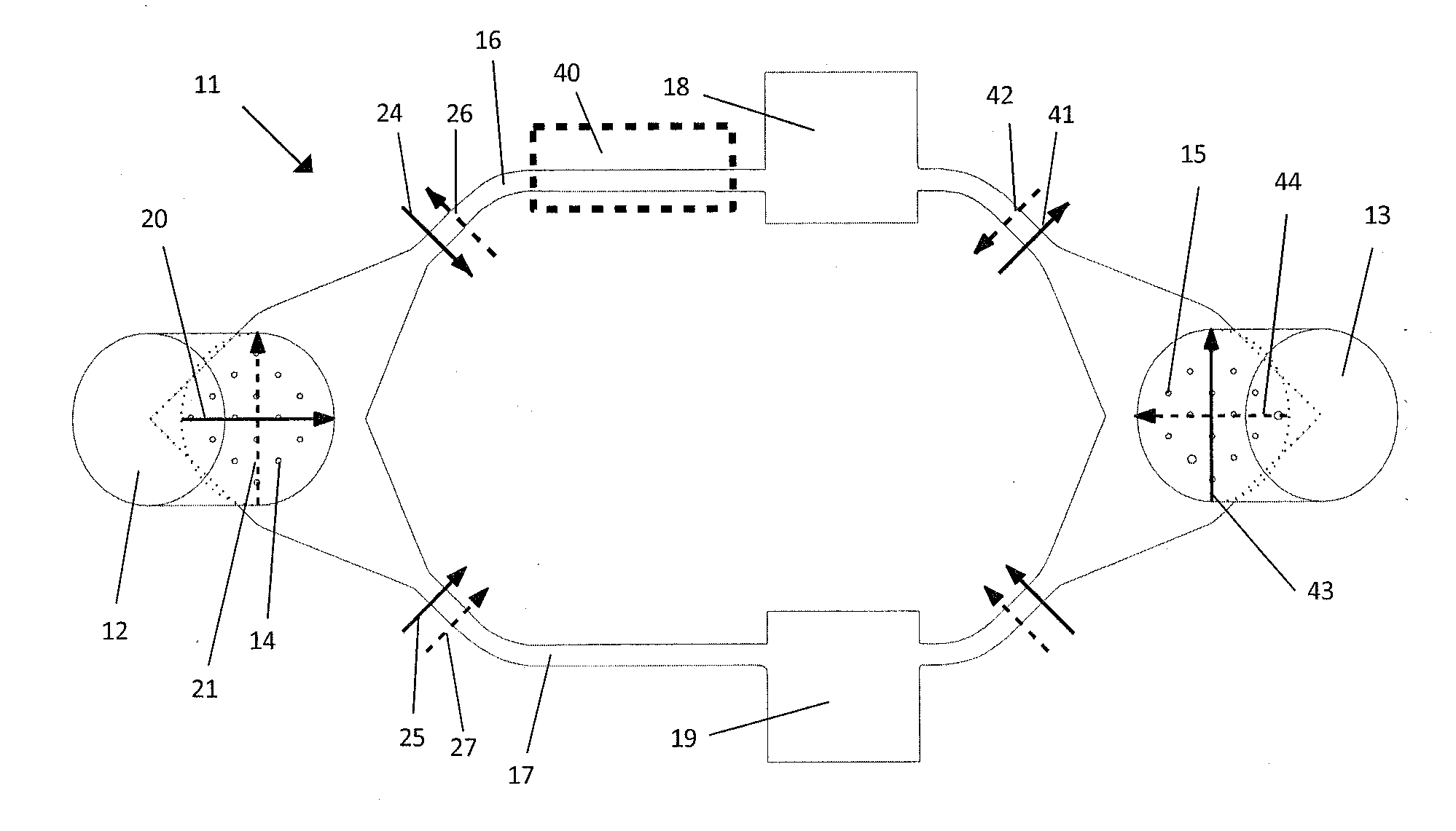
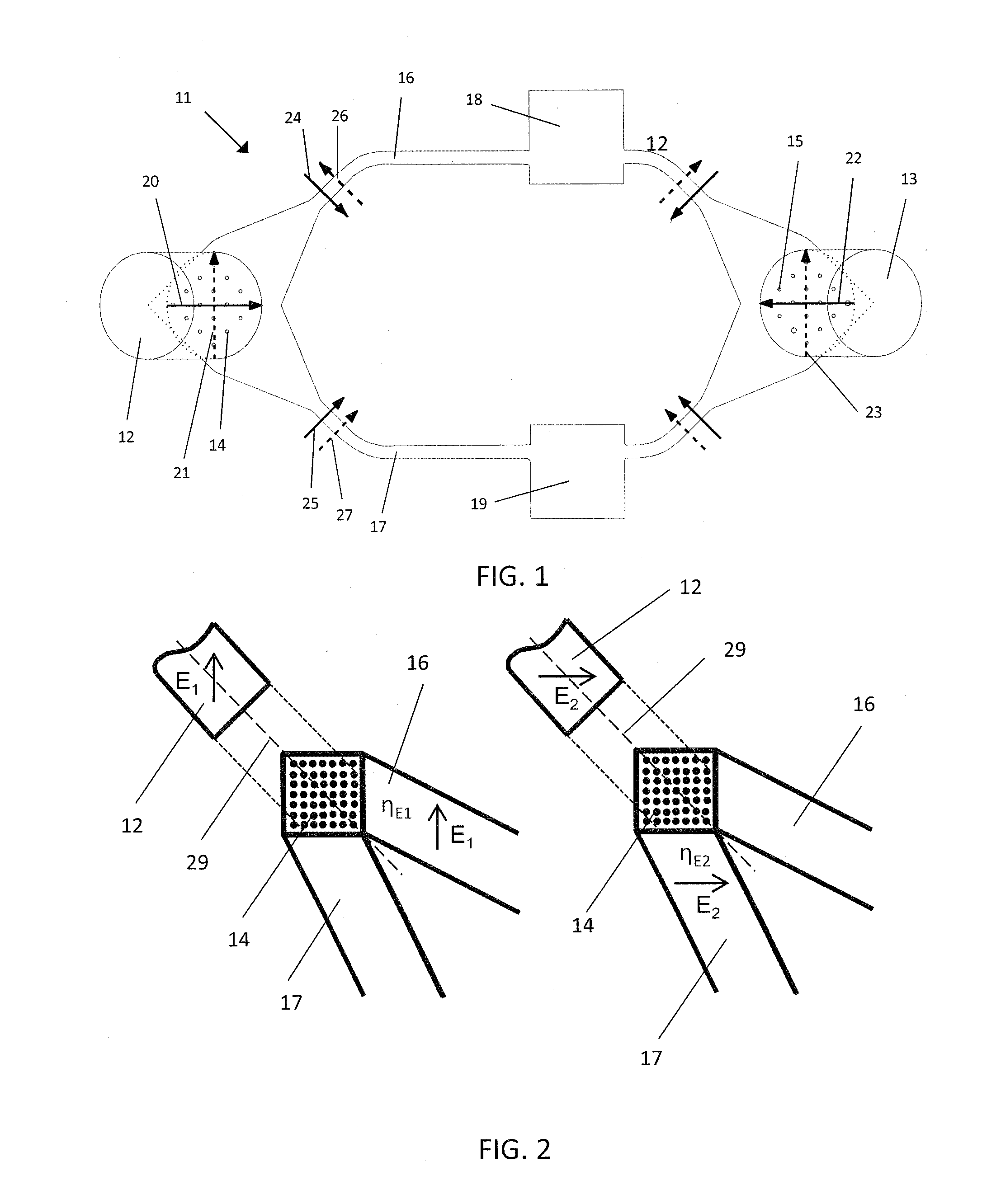
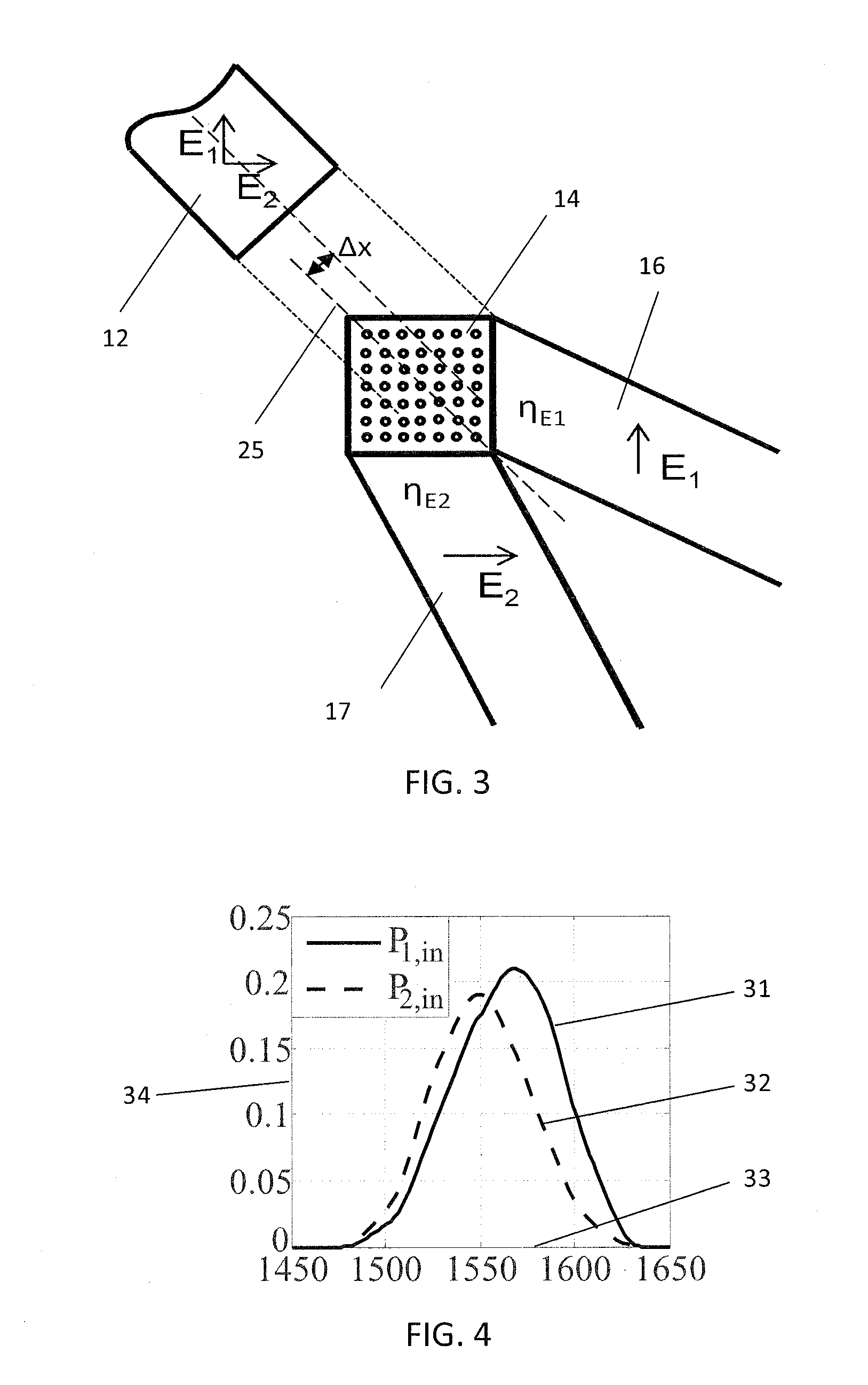
[0044]The present invention will be described with respect to particular embodiments and with reference to certain drawings but the invention is not limited thereto but only by the claims. The drawings described are only schematic and are non-limiting. In the drawings, the size of some of the elements may be exaggerated and not drawn on scale for illustrative purposes. The dimensions and the relative dimensions do not correspond to actual reductions to practice of the invention.

[0045]Furthermore, the terms first, second, third and the like in the description and in the claims, are used for distinguishing between similar elements and not necessarily for describing a sequence, either temporally, spatially, in ranking or in any other manner. It is to be understood that the terms so used are interchangeable under appropriate circumstances and that the embodiments of the invention described herein are capable of operation in other sequences than described or illustrated herein.

[0046]More...


PUM


Abstract

A photonics integrated circuit for processing radiation includes a first-dimensional grating coupler for coupling in radiation, a second two-dimensional grating coupler for coupling out radiation and a waveguide structure having two distinct waveguide arms for splitting radiation received from the first grating coupler and recombining radiation in the second grating coupler. A phase shifting means furthermore is provided for inducing an additional phase shift in at least one of the two distinct waveguide arms thereby inducing a relative phase shift of π between the two distinct waveguide arms so as to provide a TE/TM polarization switch for radiation between the first grating coupler and the second grating coupler.

Description

FIELD OF THE INVENTION[0001]This invention relates to integrated optical components and methods of operating the same. More specifically it relates to photonics integrated circuits using a two dimensional, polarization splitting, grating coupler having low or no polarization dependent loss and of methods using such systems.BACKGROUND OF THE INVENTION[0002]Photonic integrated circuits hold the potential of creating low cost, compact optical functions. The application fields in which they can be applied are very diverse: telecommunication and data communication applications, sensing, signal processing, etc. These optical circuits comprise different optical elements such as light sources, optical modulators, spatial switches, optical filters, photodetectors, etc., the optical elements being interconnected by optical waveguides. Silicon photonics is emerging as one of the most promising technologies for low cost integrated circuits for optical communication systems. It is CMOS-compatibl...

Claims


Application Information

Patent Timeline
IPC IPC(8): G02B6/12G02B6/34
CPCG02B6/29397G02B6/2793G02B6/305
Inventor ROELKENS, GUNTHERVERMEULEN, DIEDRICK
Owner UNIV GENT
Why Eureka
Try Eureka