
Silicon-Based Opto-Electronic Integrated Circuit With Reduced Polarization Dependent Loss

Active Publication Date: 2012-06-21
CISCO TECH INC
View PDF1 Cites 0 Cited by
  • Summary
  • Abstract
  • Description
  • Claims
  • Application Information

AI Technical Summary

Benefits of technology

[0009]The present invention addresses the polarization dependent loss problem associated with optical waveguides in an opto-electronic circuit arrangement by strategically placing a photodetecting device as close as possible to the entry point of the optical signal into the opto-electronic circuit arrangement. While the incoming optical signal will include both TE and TM modes, by minimizing the length of the optical waveguide path along which the signal must propagate before reaching a photodetecting device, the attenuation associated with TM mode signal will be negligible.
[0010]In one embodiment, the present invention comprises a silicon-based opto-electronic circuit formed on a silicon substrate and including at least an optical receiving component, the circuit comprising an optical waveguide formed in the silicon substrate for receiving an incoming optical signal exhibiting both transverse electric (TE) and transverse magnetic (TM) components, and a photodetecting device disposed contiguous to the optical waveguide for capturing the received optical signal and converting the received optical signal into an electrical equivalent, where the optical waveguide is configured to have a short length such that polarization dependent loss associated the TM component of the received optical signal is negligible (e.g., perhaps less than 1 dB, or less than the maximum allowable system-level tolerance to signal variation, while maintaining adequate signal integrity).
[0011]In one embodiment, the relatively short waveguide along which the mixed polarization optical signal is propagating includes a coupling scheme that comprises a nanotaper coupling end termination where the signal is introduced to the silicon substrate. A nanotaper coupling end termination may be utilized to improve the coupling efficiency between the incoming signal and the waveguide. In general, however, any suitable type of coupling scheme may be used. Additionally, it is also possible to fabricate the relatively short waveguide from the same material that used to form the photodetecting device, thus combining the functions of coupling and photodetecting.

Problems solved by technology

While such a modular component exhibits a significant improvement in reduced cost when compared to discrete element arrangements, a problem remains in that the silicon-based optical waveguides utilized in the modular are subject to polarization-dependent loss.
Obviously, the need to introduce polarization diversity optics adds cost to the final assembly.

Method used


Image

  • Silicon-Based Opto-Electronic Integrated Circuit With Reduced Polarization Dependent Loss
  • Silicon-Based Opto-Electronic Integrated Circuit With Reduced Polarization Dependent Loss
  • Silicon-Based Opto-Electronic Integrated Circuit With Reduced Polarization Dependent Loss

Examples


Embodiment Construction

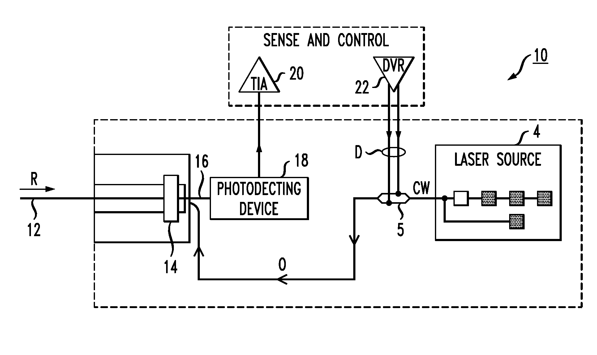
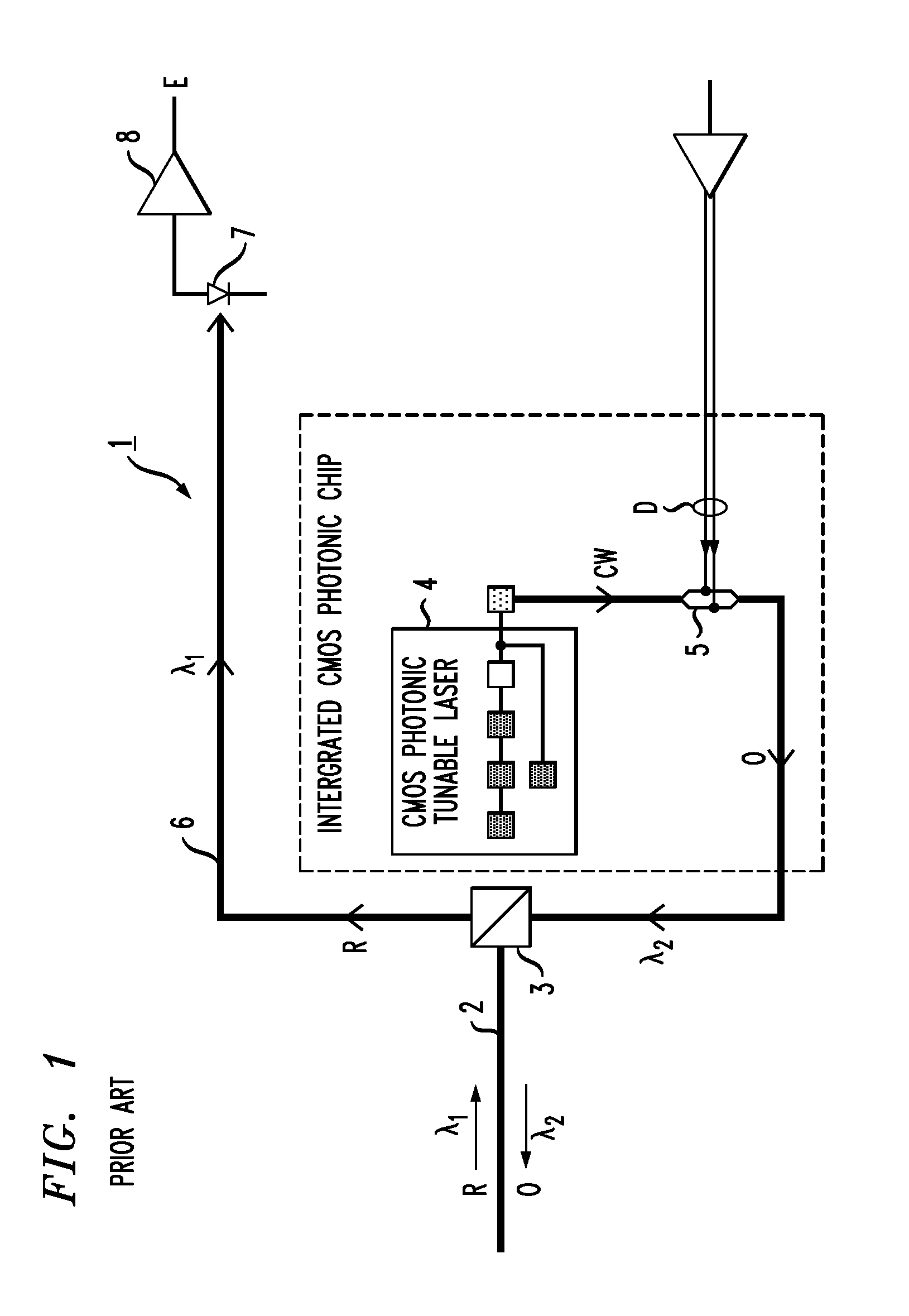
[0018]FIG. 1 illustrates an exemplary prior art opto-electronic integrated circuit 1, utilizing a single incoming optical waveguide 2 (at times, an optical fiber) to transmit optical signals between opto-electronic integrated circuit 1 and other, external components (not shown). In this particular configuration, a wavelength division multiplexer (WDM) 3 is used to separate the “incoming” / received optical signals R (operating at a first wavelength λ1) from the “outgoing” / transmitted optical signals 0 (operating at a second wavelength λ2). Opto-electronic integrated circuit 1 comprises a silicon-on-insulator (SOI)-based circuit, utilizing a silicon substrate as the platform upon which the individual components are mounted and a relatively thin (i.e., less than one micron in thickness) silicon surface layer within which optical waveguides are formed.

[0019]In a conventional manner, and not particularly relevant to the subject matter of the present invention, a tunable laser source 4 is ...


PUM


Abstract

A silicon-based opto-electronic circuit is formed to exhibit reduced polarization-dependent loss by strategically placing the photodetecting device as close as possible to the entry point of the optical signal into the opto-electronic circuit arrangement. While the incoming optical signal will include both TE and TM modes, by minimizing the length of the optical waveguide path along which the signal must propagate before reaching a photodetector, the attenuation associated with TM mode signal will be negligible.

Description

CROSS-REFERENCE TO RELATED APPLICATIONS[0001]This application claims the benefit of U.S. Provisional Application 61 / 423,432, filed Dec. 15, 2010 and herein incorporated by reference.TECHNICAL FIELD[0002]The present invention relates to a silicon-based opto-electronic integrated circuit and, more particularly, to an opto-electronic integrated circuit with reduced polarization dependent loss.BACKGROUND OF THE INVENTION[0003]Optical networking, including fiber-optics and optoelectronics, is an important aspect of high speed communication systems, particularly for its ability to allow for efficient, accurate, and rapid transmission of data between various components in the network system. As with most communication systems, the efficient use of space and power in optical networks is of ever-increasing importance. Further, design considerations for such networks must take into account the modularity of the particular components that are included in the network.[0004]Indeed, modula...

Claims


Application Information

Patent Timeline
IPC IPC(8): G02B6/12
CPCG02B6/305G02B6/421G02B6/42G02B6/4246G02B6/4213
Inventor SHASTRI, KALPENDUNERING, RAYMOND
Owner CISCO TECH INC
Learn More