Optical interconnect using optical transmitter pre-distortion

a technology of optical transmitter and optical interconnection, which is applied in the direction of optical transmission, transmission monitoring, electromagnetic transmission, etc., can solve the problems of high electrical power consumption of circuits, difficult to realize multi-mode optical devices (lasers and detectors), and difficulty in achieving amplifier circuits with sufficient raw bandwidth with acceptable power consumption, so as to improve overall link performance and reduce jitter

Active Publication Date: 2012-09-06
GLOBALFOUNDRIES US INC
View PDF5 Cites 28 Cited by
  • Summary
  • Abstract
  • Description
  • Claims
  • Application Information

AI Technical Summary

Benefits of technology

[0006]Embodiments of the invention provide a method and system for compensating for distortions introduced into an optical signal, in the operation of an optical interconnect, as the optical signal is generated, transmitted to a receiver, and converted into an electrical signal. Generally, embodiments of the invention pre-distort the optical output of an optical transmitter such that when the optical signal is received by a receiver and converted into an electrical signal, the overall link performance is improved. The link improvement is quantified through multiple parameters: data rate capability, power efficiency, sensitivity or link margin, and timing margin improvement or reduced jitter.
[0012]The optical device connected to the transmitter circuit, in one embodiment a Vertical Cavity Surface Emitting Laser (VCSEL), converts the pre-emphasized / distorted output of the circuit into a pre-emphasized / distorted optical signal, but when the transmitter optical output is presented to a bandwidth-limited receiver, the data recovered by the receiver is dramatically improved. The present invention uses transmitter equalization or pre-distortion to optimize the total link performance, that is the electrical output of the receiver and not to improve the signal quality at an intermediate point such as the transmitter output or receiver input.

Problems solved by technology

The biggest challenge for short-reach interconnects is to produce active components, namely optical transmitters and receivers, that provide sufficient bandwidth to operate at high data rates (>20 Gb / s) while maintaining low power consumption to maximize the power efficiency, commonly expressed in mW / Gb / s or pJ / bit: the energy required to transmit a bit of information.
However, as data rates have increased beyond 10 Gb / s, it is difficult to realize the multimode optical devices (lasers and detectors) and amplifier circuits with sufficient raw bandwidth with acceptable power consumption.
To achieve the highest data rates, the lasers must be operated at high current densities and the circuits typically consume high amounts of electrical power to deliver the required speed performance.

Method used


Image

  • Optical interconnect using optical transmitter pre-distortion
  • Optical interconnect using optical transmitter pre-distortion
  • Optical interconnect using optical transmitter pre-distortion

Examples


Embodiment Construction

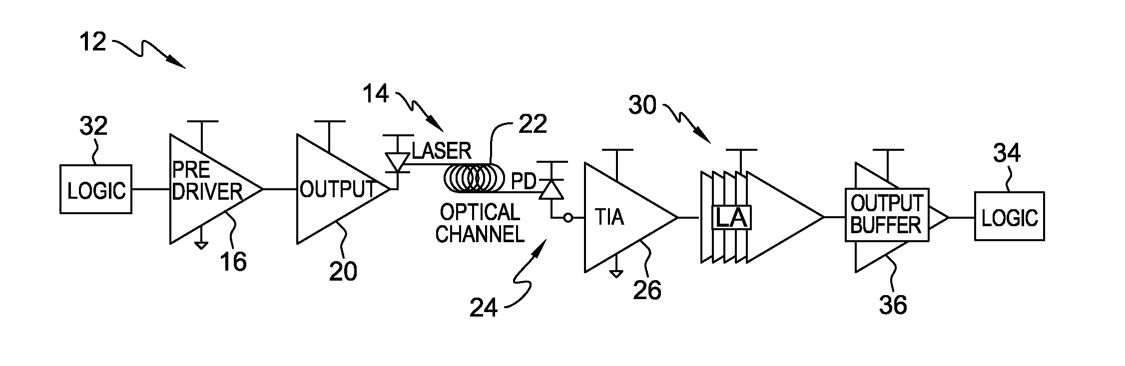
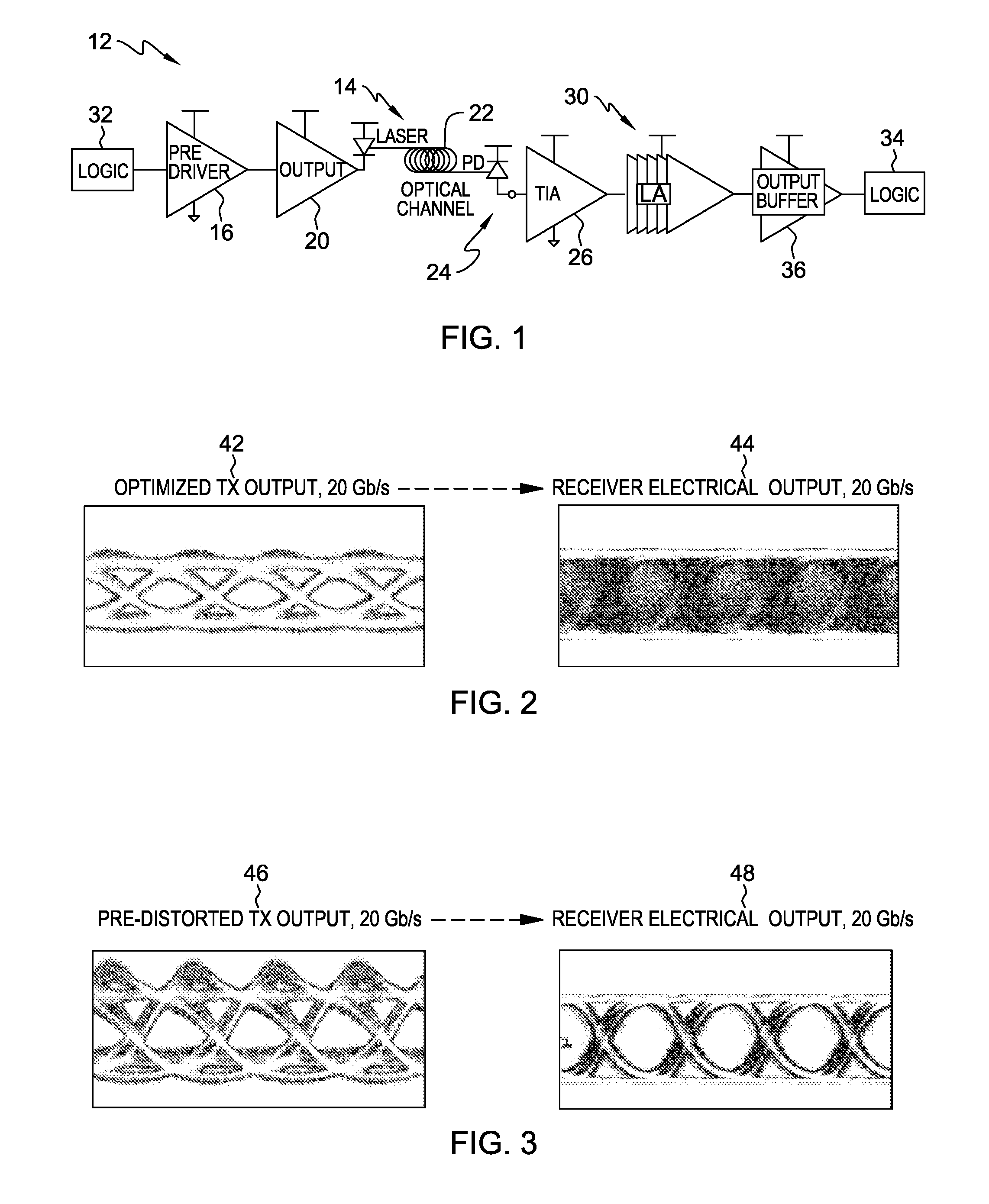
[0024]A block diagram of a typical optical data link is shown in FIG. 1. A laser diode driver 12 (LDD) converts an incoming data stream into a modulation current that is used to directly modulate the optical output of a laser 14. The laser driver is typically divided into a pre-driver stage 16 followed by an output stage 20 that directly interfaces with the laser. The modulated optical output of the laser is routed through a channel 22, typically optical fiber or optical waveguides, and coupled into an optical receiver 24. The optical receiver 24, in the embodiment shown in FIG. 1, is a photodiode that converts the incident optical signal into a small electrical current. The photodiode is connected to a transimpedance amplifier (TIA) 26 that converts the photodiode current into a voltage with some amount of gain. The TIA is followed by one or more amplifier stages 30 that provide additional gain to increase the output amplitude of the receiver to a useful level (typically 0.1-1V).

[0...


PUM


Abstract

In one embodiment, the invention provides an optical interconnect comprising a transmitter for generating and transmitting an optical signal, a receiver for receiving the optical signal from the transmitter and for converting the received optical signal to an electrical signal, and a pre-transmitter distort circuit for applying a pre-transmitter distort signal to the transmitter to adjust the shape of the optical signal generated by the transmitter. Distortions are introduced into the optical signal when the optical signal is generated, transmitted to the receiver, and converted to the electrical signal. As a result of the signal applied to the transmitter by the pre-transmitter distort circuit, the optical signal generated by the transmitter has distortions to compensate for the distortions introduced into the optical signal, wherein the electrical signal, into which the optical signal is converted, has a desired shape.

Description

BACKGROUND OF THE INVENTION[0001]This invention generally relates to fiber and waveguide optics, and more specifically, to optical interconnects in fiber optic transmissions.[0002]Fiber optics and optical interconnects are used in a wide variety of applications. The use of optical fibers as a medium for transmission of digital data (including voice data) is becoming increasingly more common due to the high reliability and large bandwidth available with optical transmission systems. In addition, optical interconnects provide for a significant increase to the available bandwidth of board-level interconnects.[0003]For example, short-reach interconnects over multi-mode optical fiber (MMF), on the order of 100 m, are widely used in computer systems, data centers, and campus networks. For these data links, the optical channel contributes relatively little signal degradation for 10-40 G data rates. In addition, generations of fiber with optimized modal bandwidth continue to be developed th...

Claims


Application Information

Patent Timeline
Patent Type & Authority Applications(United States)
IPC IPC(8): H04B10/18H04B10/08
CPCH04B10/2507H04B10/25073H04B2210/254H04B10/25137
Inventor RYLYAKOV, ALEXANDER V.SCHOW, CLINT L.
Owner GLOBALFOUNDRIES US INC
Why Eureka
Try Eureka