Large-grain, low-resistivity tungsten on a conductive compound

a technology of conductive compound and large grain, applied in the field of large grain, low resistance tungsten on a conductive compound, semiconductor and microelectronics devices, can solve the problems of increasing cost and reducing manufacturing throughpu

Inactive Publication Date: 2012-09-13
GLOBALFOUNDRIES INC
View PDF8 Cites 24 Cited by
  • Summary
  • Abstract
  • Description
  • Claims
  • Application Information

AI Technical Summary

Problems solved by technology

However, such procedures may reduce man

Method used


Image

  • Large-grain, low-resistivity tungsten on a conductive compound
  • Large-grain, low-resistivity tungsten on a conductive compound
  • Large-grain, low-resistivity tungsten on a conductive compound

Examples


Embodiment Construction

[0021]It will be readily understood that the components of the present invention, as generally described and illustrated in the figures herein, may be arranged and designed in a wide variety of different configurations in addition to the described presently preferred embodiments. Thus, the following detailed description of the embodiments of the present invention, as represented in the figures, is not intended to limit the scope of the invention, as claimed, but is merely representative of selected presently preferred embodiments of the invention. The following description is intended only by way of example, and simply illustrates certain selected presently preferred embodiments of the invention as claimed herein.

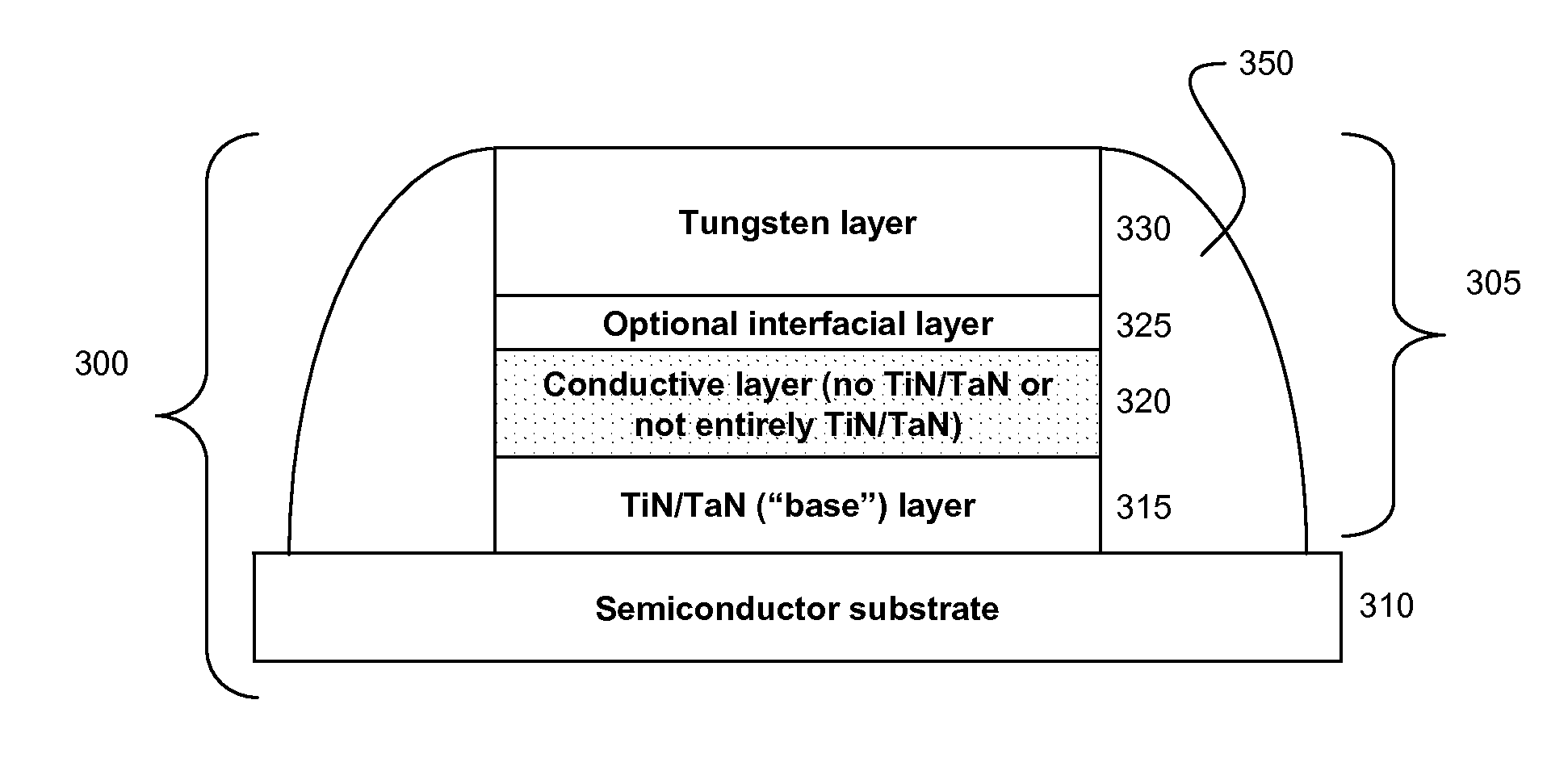
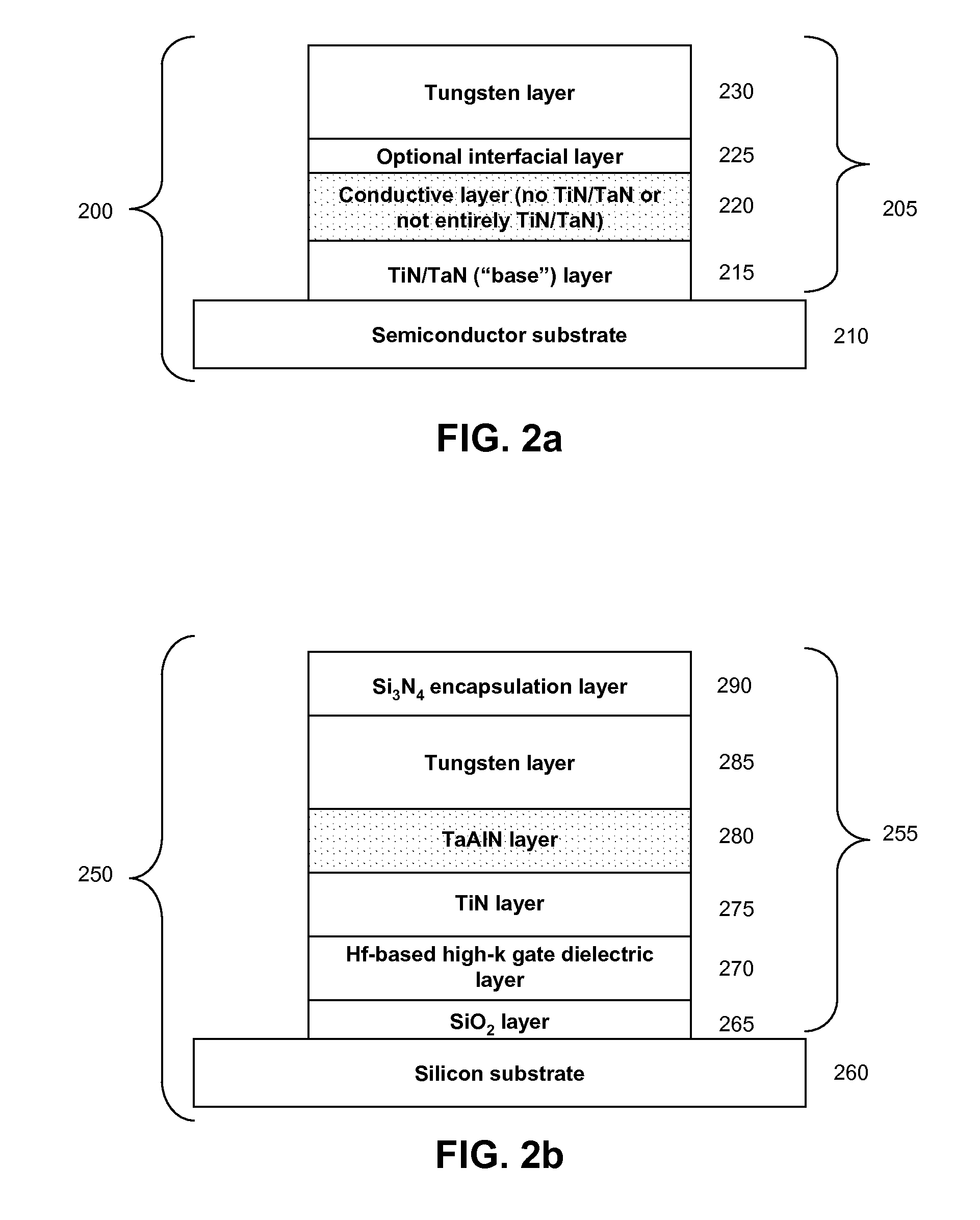
[0022]According to one embodiment of the present invention, a semiconductor device has a gate stack that includes an underlayer for a tungsten deposit. This underlayer can be a conductive layer that does not contain or is not entirely made of titanium nitride (TiN), tantalu...


PUM


Abstract

A layered structure and semiconductor device and methods for fabricating a layered structure and semiconductor device. The layered structure includes: a base layer including a material containing titanium nitride, tantalum nitride, or a combination thereof; a conductive layer including a material containing: tantalum aluminum nitride, titanium aluminum nitride, tantalum silicon nitride, titanium silicon nitride, tantalum hafnium nitride, titanium hafnium nitride, hafnium nitride, hafnium carbide, tantalum carbide, vanadium nitride, niobium nitride, or any combination thereof; and a tungsten layer. The semiconductor device includes: a semiconductor substrate; a base layer; a conductive layer; and a tungsten layer.

Description

BACKGROUND OF THE INVENTION[0001]1. Field of the Invention[0002]The present invention relates generally to semiconductor and microelectronics structures and methods for fabricating these structures. More particularly, the invention relates to semiconductor and microelectronics devices, and methods for fabricating these devices, where the device includes a conductive compound as an underlayer that allows for a tungsten deposit to form large grain size and resulting in low resistivity.[0003]2. Description of the Related Art[0004]Tungsten is a metallization element with multiple uses in electronics, and in particular in chip technology. Examples of such uses include but are not limited to using the tungsten plug fill process for filling contacts and vias in front- and back-end metallization, using tungsten as an interconnect material, using tungsten as a component of the metal-oxide-semiconductor field-effect transistor (MOSFET) gate stack, and using tungsten as a component of the dyna...

Claims


Application Information

Patent Timeline
IPC IPC(8): H01L23/48H01L21/28
CPCH01L21/28088H01L29/4966H01L29/517H01L23/53266H01L2924/0002H01L2924/00
Inventor BROWN, STEPHEN L.BRULEY, JOHNCABRAL, JR., CYRILCALLEGARI, SANDROFRANK, MARTIN M.GUILLORN, MICHAEL A.HOPSTAKEN, MARINUSNARAYANAN, VIJAYWONG, KEITH KWONG HON
Owner GLOBALFOUNDRIES INC
Why Eureka
Try Eureka