Conductive laminate and method of producing the same

a technology of conductive laminate and conductive layer, which is applied in the direction of conductive layer on insulating support, applications, other domestic articles, etc., can solve the problems of cushion layer not giving cushioning effect, production may not be achieved at low cost, and the writing sense and input sensitivity of the touch panel are improved, and the effect of favorable durability

Inactive Publication Date: 2012-09-13
TORAY IND INC
View PDF2 Cites 25 Cited by
  • Summary
  • Abstract
  • Description
  • Claims
  • Application Information

AI Technical Summary

Benefits of technology

[0014]An embodiment of the present invention is to provide a conductive laminate that can improve in writing sense and input sensitivity of a touch panel and, in addition, that can provide with favorable durability.

Problems solved by technology

However, the conductive layer is stacked by a dry process requiring high operation costs and, further, due to the configuration using multiple substrates, the cost is increasing considerably and, therefore, production may not be achieved at low cost.
Thus, even though the conductive laminate was provided with the cushion layer, the cushion layer does not give cushioning effect.
For a conductive laminate prepared by stacking a resin layer, a layer having a smaller thickness than a substrate and different index of refraction, and a conductive layer on the substrate in this sequence, writing sense and input sensitivity are poor even if the layer laminated in plural has a small thickness.
For a conductive laminate prepared by providing a base layer on a substrate and stacking a conductive layer thereon, if the base layer has a considerably smaller thickness than the substrate, the conductive laminate does not give cushioning effect and has poor writing sense and input sensitivity.
The conductive laminate with a base layer including a polyurethane resin lacks cushioning effect of the base layer and has poor writing sense and input sensitivity.
The conductive laminate with a base layer including a urethane acrylate resin lacks cushioning effect of the base layer and has poor writing sense and input sensitivity.
Specifically, a conductive layer containing a conductive component, that includes a moisture-containing composition, may incur unevenness and / or defect when it is stacked on a base resin layer, deteriorate external appearance of a conductive laminate, cause poor surface conductivity in turn entailing poor input sensitivity.

Method used


Image

  • Conductive laminate and method of producing the same
  • Conductive laminate and method of producing the same
  • Conductive laminate and method of producing the same

Examples


example 1

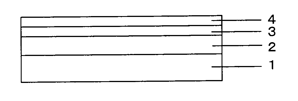
[0171]A ‘film’ having a thickness of 188 μm was used as a substrate, KAYANOVA (registered trademark) FOP 1740 (manufactured by Nippon Kayaku Co., Ltd., solid content of 82% by weight) was diluted with toluene and methylethylketone at a ratio by weight of 1:1, to the solid content of 40% by weight and hence prepare a hard coating agent, the hard coating agent was applied to one face of the substrate by a micro-gravure coater (gravure line No. 80R, gravure rotation rate 100%) and dried at 80° C. for 1 minute, followed by UV irradiation at 1.0 J / cm2 and curing to thereby form a hard coating layer having a thickness of 5 μm.

[0172]Next, 1.40 g of ‘resin A’, 13.85 g of ‘resin B’, and 2.00 g of ethyl acetate were mixed and agitated to prepare a base resin layer coating solution. Using a bar coater No. 30 (manufactured by Matsuo Sangyo Co., Ltd.), the coating solution was applied to the other face opposed to the face of the substrate, on which the hard coating layer was provided, followed b...

example 2

[0174]Except that a base resin layer coating solution has the constitutional composition of; 1.40 g of ‘resin A’, 13.96 g of ‘resin B’, 0.041 g of ‘photo-polymerization initiator’, and 2.08 g of ethyl acetate and, after applying and drying a coating solution, UV ray was radiated at 1.2 J / cm2, the sample procedure as described in Example 1 was executed and ‘conductive layer A’ was stacked on the base resin layer having a coating thickness of 13 μm after drying, by gravure line No. 150R, thus resulting in a conductive laminate.

example 3

[0175]A ‘film’ having a thickness of 188 μm was used as a substrate, KAYANOVA (registered trademark) FOP 1740 (manufactured by Nippon Kayaku Co., Ltd., solid content of 82% by weight) was diluted with toluene and methylethylketone at a ratio by weight of 1:1, to the solid content of 40% by weight and hence prepare a hard coating agent, the hard coating agent was applied to one face of the substrate by a micro-gravure coater (gravure line No. 80R, gravure rotation rate 100%) and dried at 80° C. for 1 minute, followed by UV irradiation at 1.0 J / cm2 and curing to thereby form a hard coating layer having a thickness of 5 μm.

[0176]Next, 3.48 g of ‘resin A’, 8.92 g of ‘resin B’, and 7.59 g of ethyl acetate were mixed and agitated to prepare a base resin layer coating solution. Using a bar coater No. 30 (manufactured by Matsuo Sangyo Co., Ltd.), the base resin layer coating solution was applied to the other face opposed to the face of the substrate, on which the hard coating layer was prov...


PUM

PropertyMeasurementUnit
luminous transmittanceaaaaaaaaaa
transparencyaaaaaaaaaa
thicknessaaaaaaaaaa

Abstract

Provided is a conductive laminate comprising a base resin layer and a conductive layer on at least one surface of a substrate, by stacking in the sequential order of the base resin layer and the conductive layer from the substrate side, and in which the base resin layer comprises a resin including a urethane acrylate resin having a glycol skeleton, and a grafted resin having a hydrophilic group among side chains thereof. A touch panel using the conductive laminate of the present invention exhibits good writing sense, high input sensitivity and favorable durability. In addition, the conductive laminate of the present invention is preferably used for electrode members, which are employed in display products such as a liquid crystal display, an organic electro-luminescence, and an electronic paper as well as solar cell modules, and so forth.

Description

CROSS REFERENCE TO RELATED APPLICATION[0001]This application is the U.S. National Phase application of PCT International Application No. PCT / JP2010 / 069405, filed Nov. 1, 2010, and claims priority to Japanese Patent Application No. 2009-257833, filed Nov. 11, 2009, the disclosures of which PCT and priority applications are incorporated herein by reference in their entireties for all purposes.FIELD OF THE INVENTION[0002]The present invention relates to a conductive laminate having a conductive layer on a base resin layer. More particularly, the present invention relates to a conductive laminate suitable for an electrode member used in a solar cell module and a display product such as a touch panel, a liquid crystal display, an organic electroluminescence, and an electronic paper.BACKGROUND OF THE INVENTION[0003]In recent years, a mobile phone, a game console, and the like, including a touch panel mounted thereon, have been propagated. The touch panel may be fabricated using a conducti...

Claims


Application Information

Patent Timeline
Patent Type & Authority Applications(United States)
IPC IPC(8): B32B9/04B05D5/12B32B27/40B32B7/02B82Y30/00B82Y40/00
CPCB32B27/308Y10T428/2495B32B2457/208B32B2307/202Y10T428/31551B32B27/40H01B5/14H01B13/00
Inventor SATO, YOSHIKAZUWATANABE, OSAMU
Owner TORAY IND INC
Why Eureka
Try Eureka