Predictive link processing

a technology of pre-determined link and processing method, which is applied in the direction of solid-state device details, semiconductor/solid-state device components, manufacturing tools, etc., can solve the problems of increasing the time required to process a given die, increasing the difficulty of link removal, and increasing the difficulty of irradiating a target structure without damaging surrounding components

Inactive Publication Date: 2012-09-27
ELECTRO SCI IND INC
View PDF0 Cites 15 Cited by
  • Summary
  • Abstract
  • Description
  • Claims
  • Application Information

AI Technical Summary

Benefits of technology

[0029]In another system for processing selected material by laser interaction where the material distributed at locations about a workpiece, the system may include a laser source configured to generate a pulsed laser processing output along a laser beam axis, one or more beam deflectors defining a deflection field, means for moving the workpiece relative to the deflection field; and a system controller. The system controller may be configured to store data representative of a selected processing field shape that comprises a portion of the deflection field, store timing data representative of a laser pulse that can be emitted for processing material, store data representative of one or more workpiece locations selected for processing, predict the position of the one or more workpiece locations selected for processing on the moving workpiece within the deflection field at one or more laser pulse times based on the stored timing data, compare the predicted position of the one or more workpiece locations with the selected field shape, and prevent laser interaction at any one of the one or more workpiece locations that is not within the selected field shape.
[0030]In another such system, the system may include a laser source configured to generate a pulsed laser processing output along a laser beam axis, one or more beam deflectors defining a deflection field, means for moving the workpiece relative to the deflection field, and a system controller. The system controller may be configured to store data representative of a selected processing field shape that comprises a portion of the deflection field, store data representative of one or more workpiece locations selected for processing, move the workpiece relative to the deflection field, compare the position of the one or more workpiece locations in the deflection field with the selected field shape, and prevent laser interaction at any one of the one or more workpiece locations that is not within the selected field shape.

Problems solved by technology

Recently, the use of new materials, such as aluminum, gold, and copper, coupled with the small geometry of these devices, have made the problem of link removal more difficult.
Thus, it can be increasingly difficult to irradiate a target structure without damaging surrounding components such as the substrate and adjacent circuitry and links.
Furthermore, as more links need to be processed for a given area of semiconductor circuitry, the time required to process a given die increases.

Method used


Image

  • Predictive link processing
  • Predictive link processing
  • Predictive link processing

Examples


Embodiment Construction

Overview

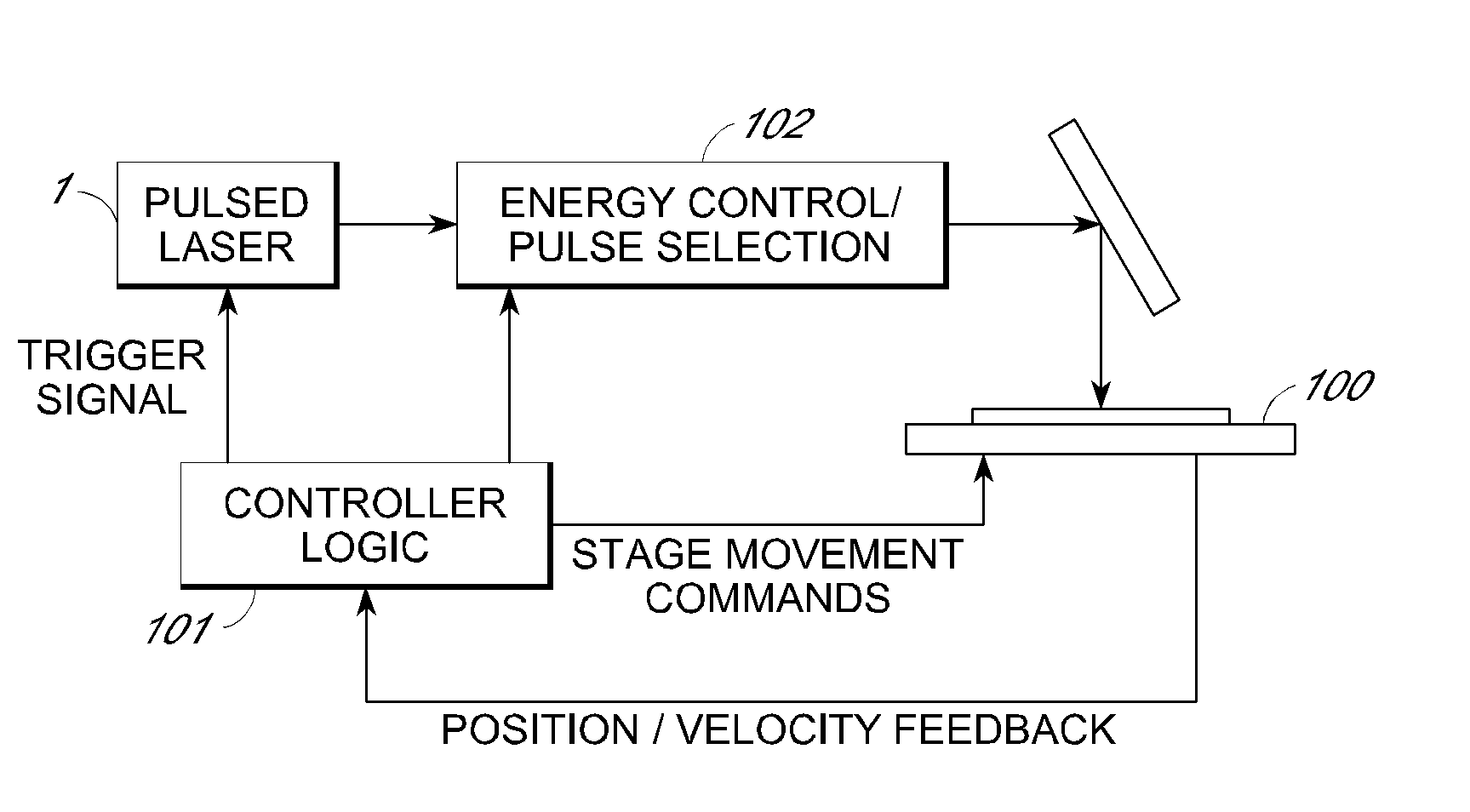
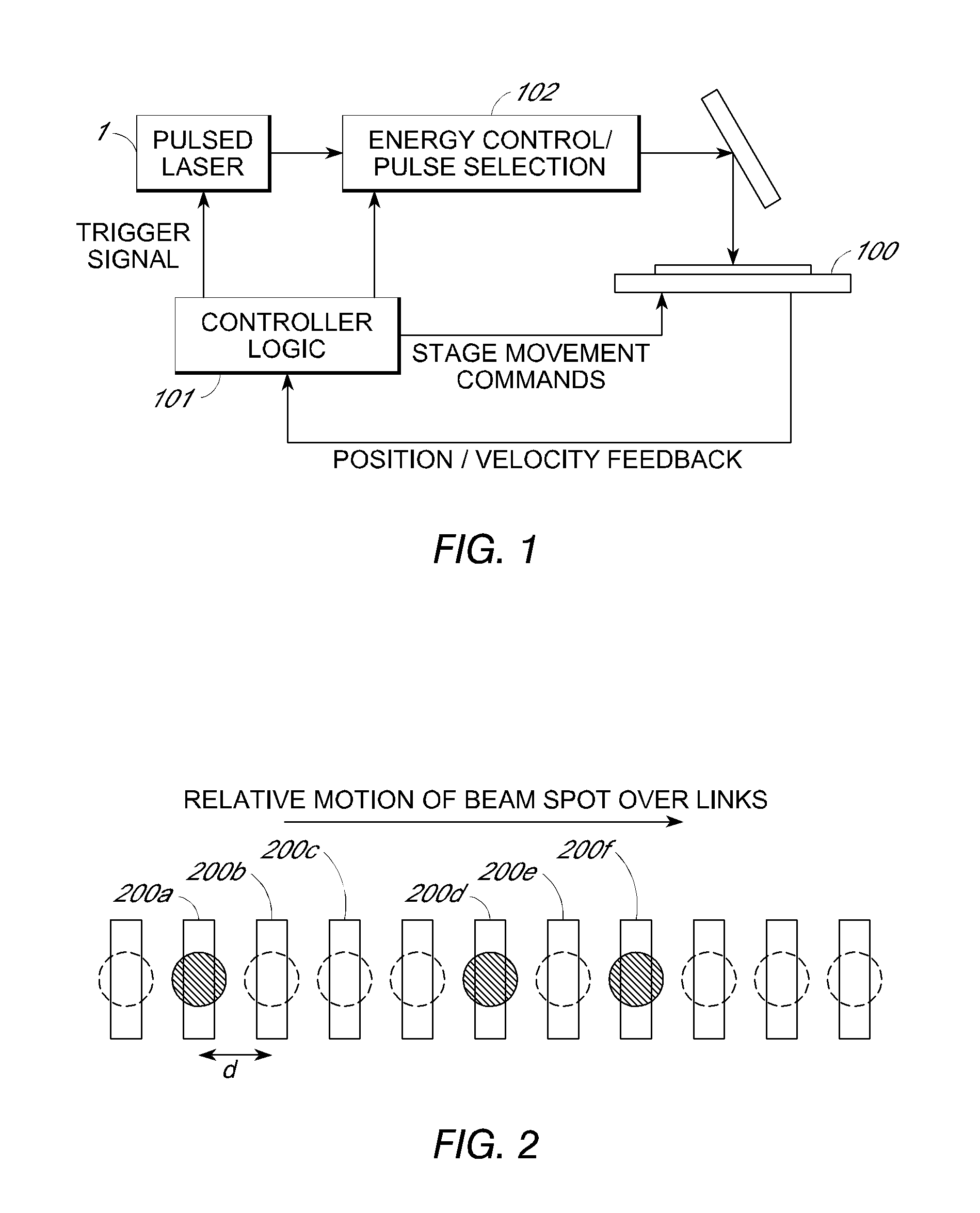
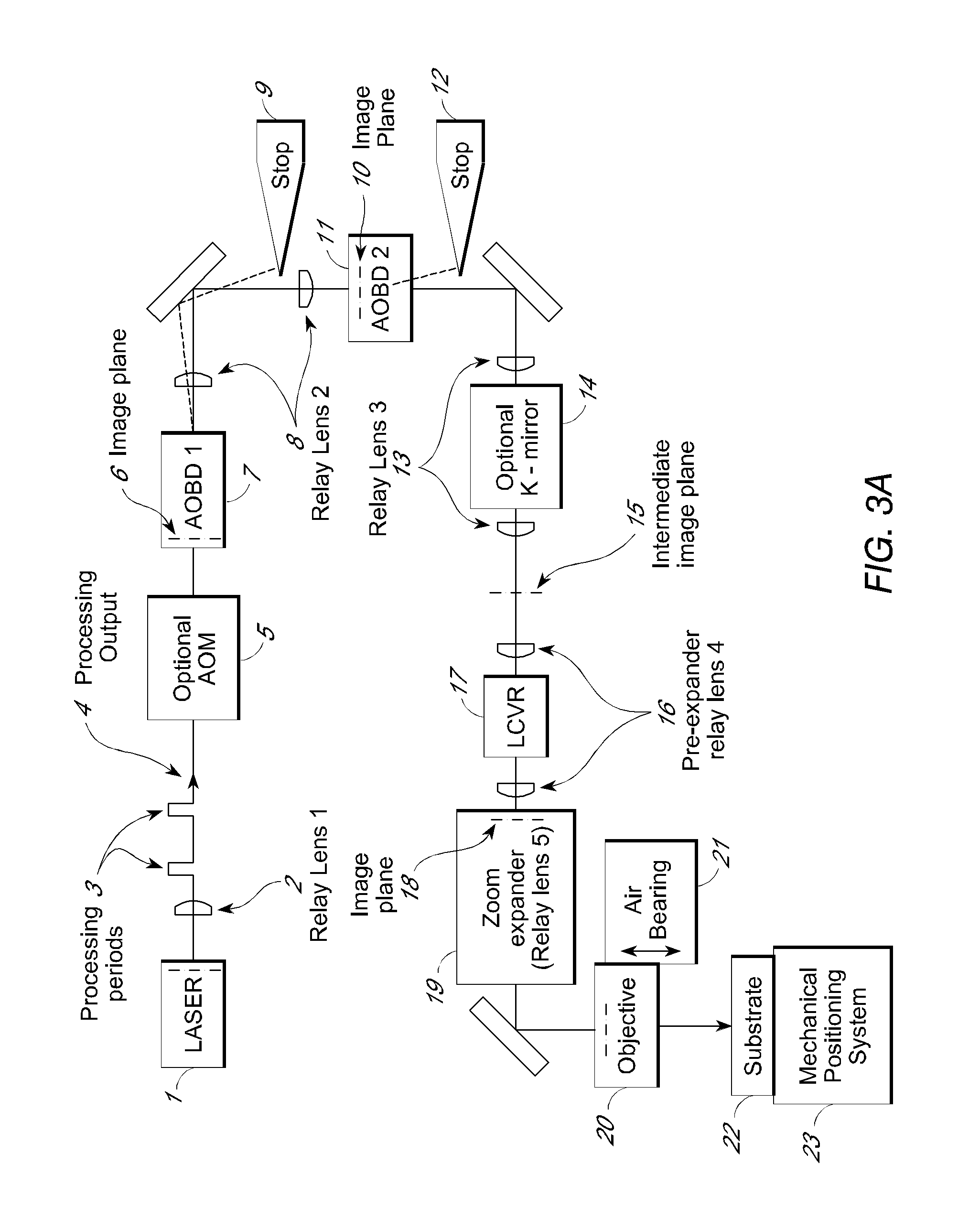
[0059]Multi-axis inertialess beam positioning is used to access processing targets relative to the trajectory of a mechanical positioning system to sever conductive links at high rates. Various laser processing aspects using split and / or deflected beams are disclosed in US patent publication 20090095722. This document is incorporated herein by reference and forms part of this application. The present disclosure is primarily directed to rapid access with a single beam. In particular, the approach uses high speed positioning within a two dimensional random access field that moves along a trajectory relative to the wafer. Positioning laser spots within the field at a processing rate allows flexible access to links passing through the field along the trajectory with a throughput exceeding a conventional link pitch based processing rate. Elapsed time traditionally required for passing over unprocessed links can be reduced, a higher percentage of laser pulses are used for processi...


PUM

PropertyMeasurementUnit
widthaaaaaaaaaa
sizeaaaaaaaaaa
diameteraaaaaaaaaa

Abstract

A method of processing material of device elements by laser interaction is disclosed. According to one aspect, the method includes generating a pulsed laser processing output along a laser beam axis, the output including a plurality of laser pulses triggered sequentially at times determined by a pulse repetition rate. A trajectory relative to locations of device elements to be processed is generated. A position of one or more designated device elements relative to an intercept point position on the trajectory at one or more laser pulse times is determined, and a laser beam is deflected based on the predicted position within a predetermined deflection range. According to some aspects, the predetermined deflection range may correspond to a compass rose or cruciform field shape. As a result, a deflection accuracy for laser processing may be improved.

Description

CROSS REFERENCE TO RELATED APPLICATIONS[0001]This application is a Continuation-In-Part of U.S. application Ser. No. 12 / 976,539, entitled Link Processing with High Speed Beam Deflection, filed on Dec. 22, 2010, which application claims priority to U.S. Provisional Application 61 / 291,282, filed on Dec. 30, 2009. This application also claims priority to U.S. Provisional Application 61 / 446,943, filed on Feb. 25, 2011.BACKGROUND OF THE INVENTION[0002]1. Field of the Invention[0003]The present invention relates to the field of laser processing methods and systems, and specifically, to laser processing methods and systems for laser processing multi-material devices.[0004]2. Description of the Related Art[0005]Lasers can be used in the processing of microstructures in memory and integrated circuit devices. For example, laser pulses can be used to ablate conductive links or link portions in a memory device, such as DRAMs in order to substitute working redundant memory cells for defective me...

Claims


Application Information

Patent Timeline
Patent Type & Authority Applications(United States)
IPC IPC(8): B23K26/00
CPCB23K26/041B23K26/0621B23K26/063H01L23/5258B23K26/0807H01L21/76892B23K26/0732B23K26/042B23K26/0619B23K26/0622B23K26/082H01L2924/0002H01L2924/00
Inventor MALTSEV, DIMITRYROMASHKO, DMITRY N.PLOTKIN, MICHAELEHRMANN, JONATHAN S.CORDINGLEY, JAMES J.
Owner ELECTRO SCI IND INC
Why Eureka
Try Eureka