Substrate cleaning apparatus and vacuum processing system

Active Publication Date: 2012-10-04
TOKYO ELECTRON LTD +1
View PDF59 Cites 184 Cited by
  • Summary
  • Abstract
  • Description
  • Claims
  • Application Information

AI Technical Summary

Benefits of technology

[0009]In the present invention, the unnecessary substances of the peripheral portion of the substrate is removed by supplying the cleaning gas clusters (aggregates of atoms and/or molecules) generated by injecting the cleaning gas from the nozzle unit in a processing atmosphere having a pressure lower than that in the nozzle unit while relatively moving

Problems solved by technology

Since a plasma is not ejected on the peripheral portion of the backside of the wafer, a reaction product, e.g., polymer, generated by the reaction between the laminated films and the plasma on the wafer surface is deposited thereon, and thus undesired particles may be generated.
Acute silicon irregularities (the protrusions of needle shape) formed at the peripheral portion of the wafer surface are not easily removed by plasma cleaning due to the anisotropic property of the pla

Method used


Image

  • Substrate cleaning apparatus and vacuum processing system
  • Substrate cleaning apparatus and vacuum processing system
  • Substrate cleaning apparatus and vacuum processing system

Examples


Embodiment Construction

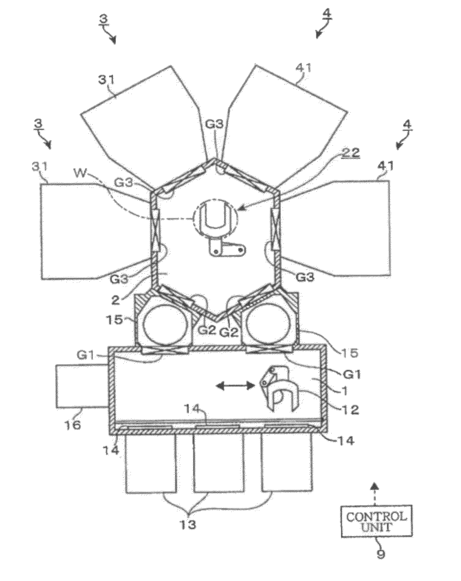
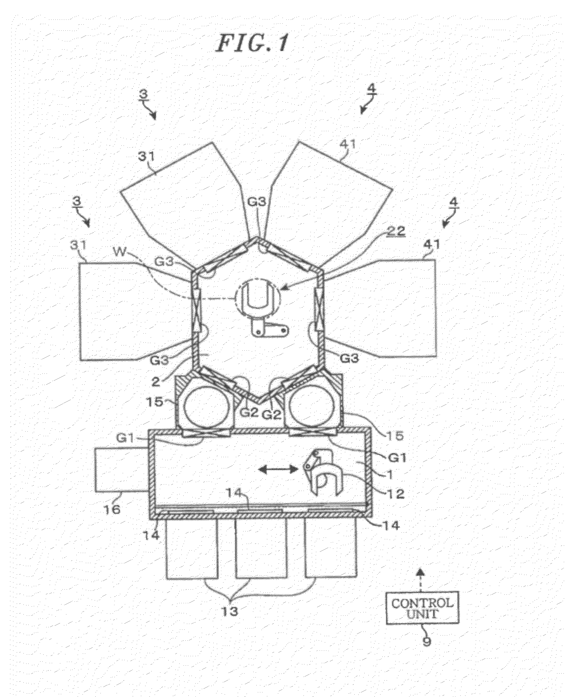
[0022]FIG. 1 shows a vacuum processing system having a substrate cleaning apparatus 4 in accordance with an embodiment of the present invention. The vacuum processing system includes an atmospheric transfer chamber 1 having a rectangular shape when seen from above. A loading / unloading port for loading and unloading a semiconductor (silicon) wafer is provided at one longitudinal side of the atmospheric transfer chamber 1. The loading / unloading port has a plurality of loading / unloading stages 13 for mounting thereon a FOUP (front opening unified pod) as a transfer container for accommodating a plurality of wafers W and doors 14 provided for the loading / unloading stages 13.

[0023]A vacuum transfer chamber 2 having a hexagonal shape when seen from above is connected, via a right and a left load-lock chamber 15 (preliminary vacuum chambers), to the other side of the atmospheric transfer chamber 1 which is opposite to the side where the loading / unloading stage 13 is provided. Connected to ...


PUM

PropertyMeasurementUnit
Pressureaaaaaaaaaa
Angleaaaaaaaaaa

Abstract

A substrate cleaning apparatus includes a supporting unit, provided in a processing chamber having a gas exhaust port, for supporting a substrate; one or more nozzle units, each for ejecting gas clusters to a peripheral portion of the substrate supported by the supporting unit to remove unnecessary substances from the peripheral portion; and a moving mechanism for changing relative positions of the supporting unit and the nozzle unit during ejecting the gas clusters. Each nozzle unit discharges a cleaning gas having a pressure higher than that in the processing chamber so that the cleaning gas is adiabatically expanded to form aggregates of atoms and/or molecules.

Description

CROSS-REFERENCE TO RELATED APPLICATIONS[0001]This application claims priority to Japanese Patent Application No. 2011-080098 filed on Mar. 31, 2011, the entire contents of which are incorporated herein by reference.FIELD OF THE INVENTION[0002]The present invention relates to a technique for cleaning a peripheral portion of a substrate.BACKGROUND OF THE INVENTION[0003]In a semiconductor device manufacturing process, a process for forming a hole or a trench in laminated films formed on a semiconductor wafer (hereinafter, referred to as a “wafer”) through a resist mask formed on the laminated films by using single etching apparatus is being examined, in which an etching gas corresponding to each film is employed. In such process, after the laminated films are formed on the wafer, a peripheral portion thereof is removed by a wet cleaning apparatus and, then, a resist pattern is formed on the remaining laminated films. Therefore, when the wafer is etched, silicon as a base material is ex...

Claims


Application Information

Patent Timeline
IPC IPC(8): C23F1/08A47L9/08A47L5/00
CPCH01L21/67051H01L21/67028C23C16/45563C23C16/45574C23C16/45582C23C16/45587H01J37/321H01J37/3244H01J37/32449H01L21/67069
Inventor DOBASHI, KAZUYAINAI, KENSUKESHIMIZU, AKITAKAYASUDA, KENTAYOSHINO, YUAIDA, TOSHIHIROSENOO, TAKEHIKO
Owner TOKYO ELECTRON LTD
Why Eureka
Try Eureka