Monolithic ceramic capacitor

a ceramic capacitor and monolithic technology, applied in the field of monolithic ceramic capacitors, can solve the problems of delamination, more likely to occur structural defects, and more likely to occur cracks during firing, and achieve the effect of small size and high performan

Active Publication Date: 2012-10-04
MURATA MFG CO LTD
View PDF3 Cites 33 Cited by
  • Summary
  • Abstract
  • Description
  • Claims
  • Application Information

AI Technical Summary

Benefits of technology

[0010]In various preferred embodiments of the present invention, among the ceramic layers, the number N of the ceramic layers disposed between the first inner electrodes and the second inner electrodes is preferably at least 232, for example. Thus, the monolithic ceramic capacitor according to preferred embodiments of the present invention includes a large number of the stacked ceramic layers and exhibits higher performance while having a small size. Further, the proportion of volume occupied by the first and second inner electrodes in the ceramic sintered body is preferably at least about 0.37, for example. Still further, the size of the side gap portion in the widthwise direction is preferably about 40 μm or less, for example. As a result, the monolithic ceramic capacitor according to preferred embodiments of the present invention is less susceptible to cracks.

Problems solved by technology

However, when trying to satisfy those requirements, a problem arises in that structural defects, such as cracks and delamination, are more likely to occur during firing.
However, the monolithic ceramic capacitor including ceramic layers, which are thinner and are stacked in a larger number, has a problem in that cracks are more likely to occur when thermal shocks is applied during, e.g., soldering.

Method used


Image

  • Monolithic ceramic capacitor
  • Monolithic ceramic capacitor
  • Monolithic ceramic capacitor

Examples


experimental examples

[0051]The ceramic capacitor 1 according to the above-described preferred embodiment was fabricated using the same materials under the conditions indicated in Tables 1 to 3, below, in 300 samples for each set of conditions.

[0052]Among the various dimensions indicated in Tables 1 to 3, the length, the width, and the thickness of the ceramic sintered body were measured by an optical microscope (MEASURESCOPE MM-10 made by Nikon Corporation) at a magnification of 50 and accuracy of ±0.01 mm. The thickness of the ceramic layer and the thickness of the inner electrode were measured by a scanning electron microscope (JSM-5800 made by JOEL Ltd.) at an acceleration voltage of 20 kV, a magnification of 15000, and accuracy of ±0.01 μm. The other dimensions were measured by an optical microscope at a magnification of 500 and accuracy of ±0.001 mm.

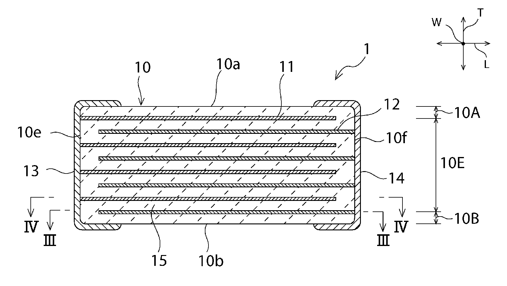
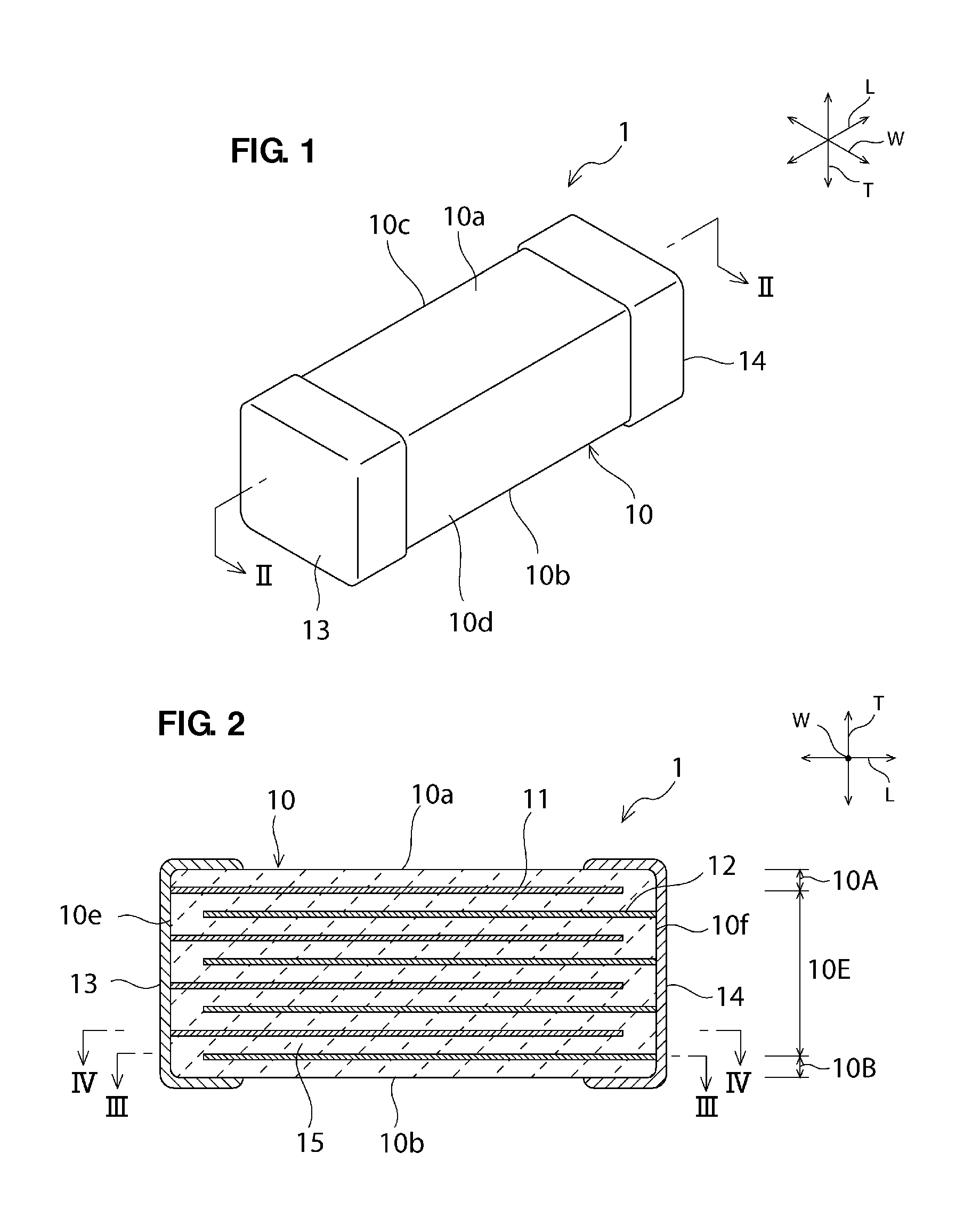
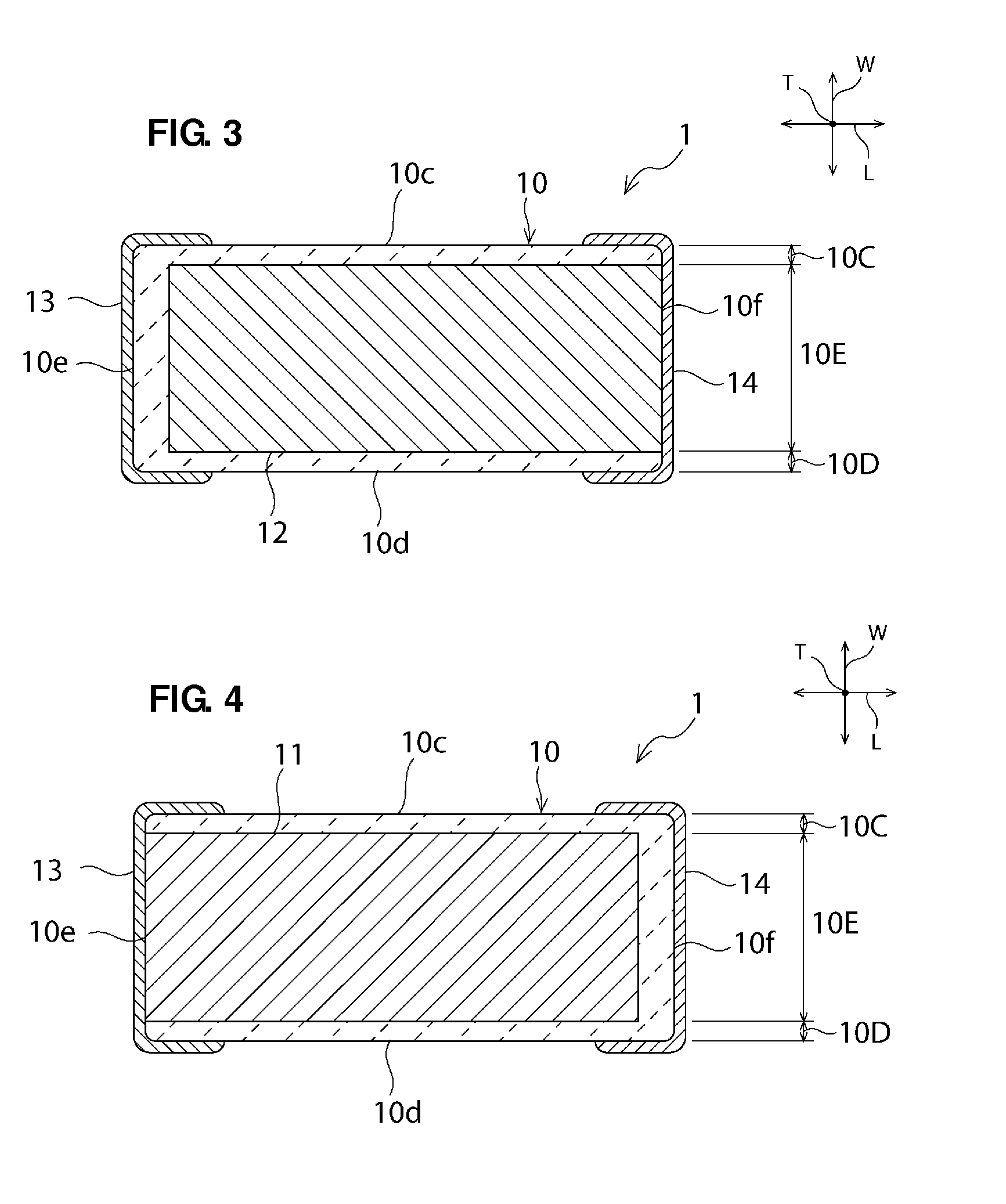
[0053]The distance from the end of the inner electrode to the outer electrode was measured at a central portion of the capacitor in the widthwise direc...


PUM

PropertyMeasurementUnit
sizeaaaaaaaaaa
thicknessaaaaaaaaaa
thicknessaaaaaaaaaa

Abstract

A monolithic ceramic capacitor includes a ceramic sintered body including a plurality of stacked ceramic layers, and first and second inner electrodes alternately arranged inside the ceramic sintered body to oppose each other in a stacking direction of the ceramic layers with the ceramic layers interposed between the adjacent first and second inner electrodes. Among the ceramic layers, a number N of the ceramic layers disposed between the first inner electrodes and the second inner electrodes is at least 232. A proportion of volume occupied by the first and second inner electrodes in the ceramic sintered body is at least about 0.37. A size of each of side gap portions is about 40 μm or less.

Description

BACKGROUND OF THE INVENTION[0001]1. Field of the Invention[0002]The present invention relates to a monolithic ceramic capacitor. In particular, the present invention relates to a monolithic ceramic capacitor including a ceramic sintered body, and a plurality of first and second inner electrodes that are alternately arranged inside the ceramic sintered body so as to be opposed to each other with a ceramic layer interposed between the adjacent first and second inner electrodes.[0003]2. Description of the Related Art[0004]Previously, monolithic ceramic capacitors, for example, have been used in many electronic devices, such as cellular phones and notebook personal computers.[0005]With a recent trend toward smaller sizes and higher performance of electronic devices in which monolithic ceramic capacitors are mounted, monolithic ceramic capacitors having smaller sizes and higher capacities have been developed. As large-capacity capacitors of 10 μF to 100 μF, for example, an aluminum elect...

Claims


Application Information

Patent Timeline
Patent Type & Authority Applications(United States)
IPC IPC(8): H01G4/30
CPCH01G4/012H01G4/30H01G4/12
Inventor FUKUNAGA, DAIKIOKAJIMA, KENICHIYAMASHITA, YASUHARUMURANISHI, NAOTOTANAKA, HIDEAKI
Owner MURATA MFG CO LTD
Why Eureka
Try Eureka