

Semiconductor device and method for manufacturing the same
a semiconductor film and semiconductor technology, applied in the direction of semiconductor devices, basic electric elements, electrical appliances, etc., can solve the problems of large leakage current between the source and the drain of the transistor, adverse effects on the electric characteristics of the transistor, and the inability to form over a larger glass substrate, etc., to achieve the reduction of the oxygen vacancy in the oxide semiconductor film, and the reduction of the negative shift of the threshold voltage of the transistor
- Summary
- Abstract
- Description
- Claims
- Application Information
AI Technical Summary
Benefits of technology
Problems solved by technology
Method used
Image

Examples
embodiment 1
)
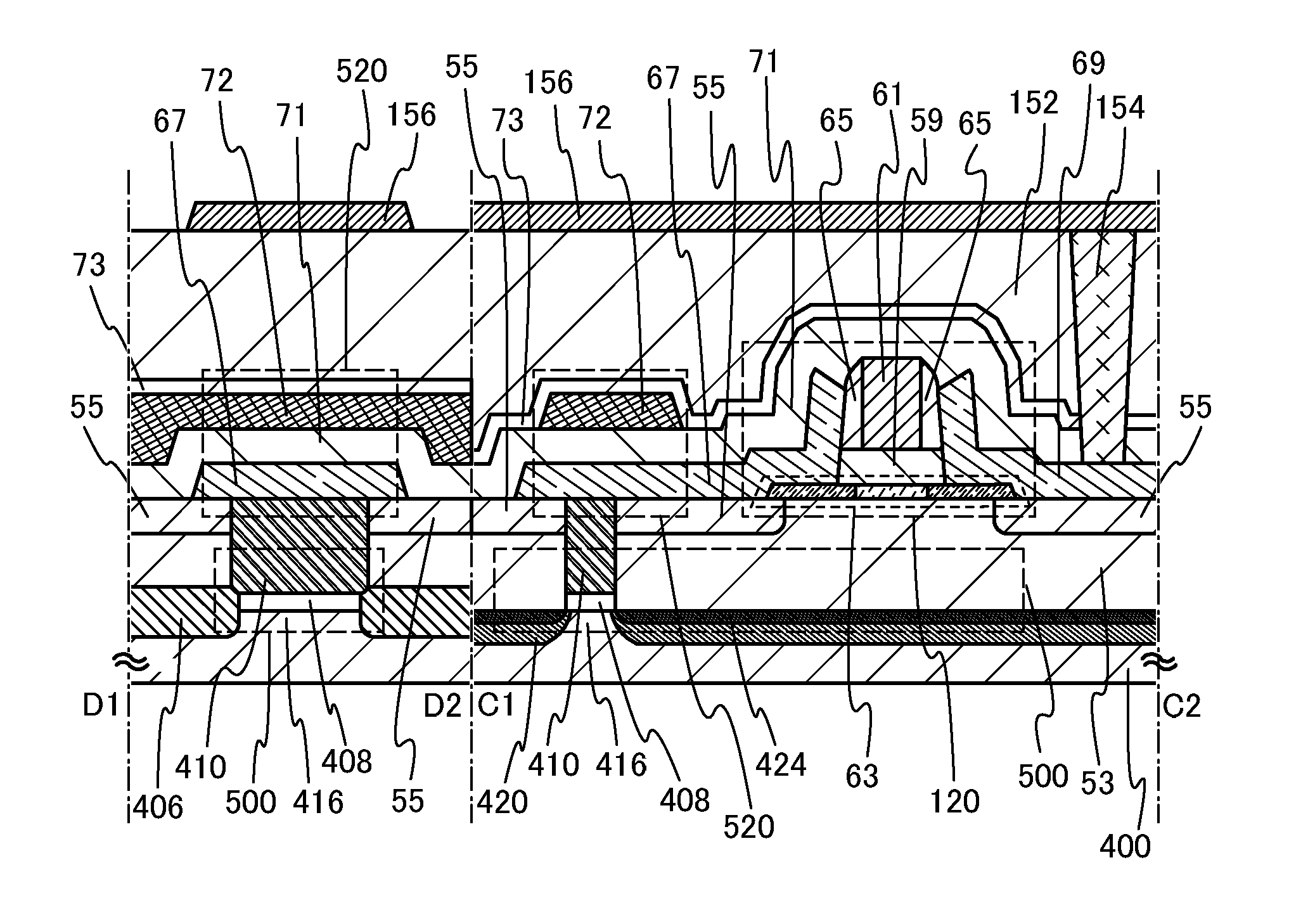
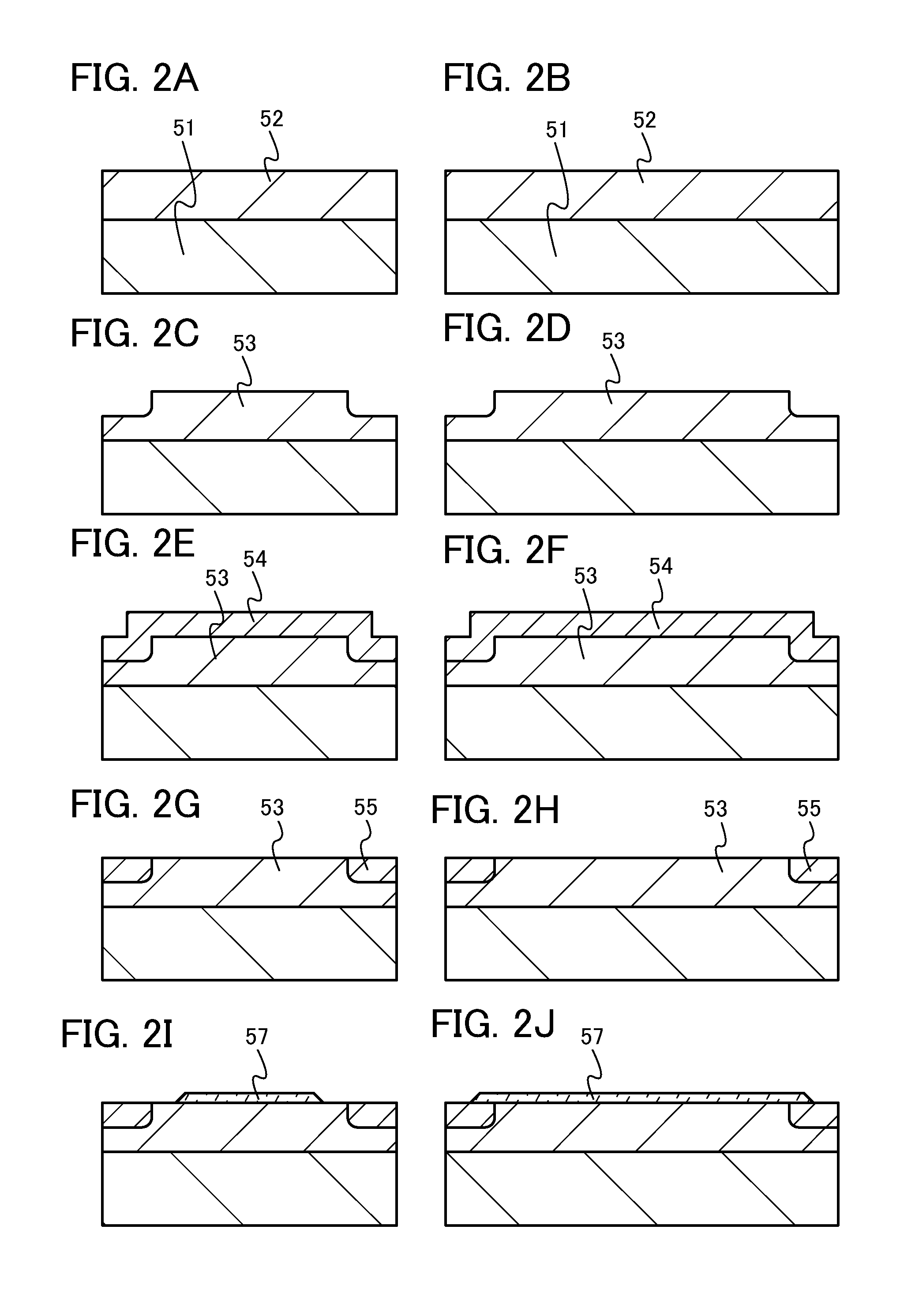
[0035]In this embodiment, a structure of a transistor in which a leakage current can be reduced and a manufacturing method of the transistor will be described with reference to FIGS. 1A to 1C, FIGS. 2A to 2J, FIGS. 3A to 3H, and FIGS. 4A to 4F.
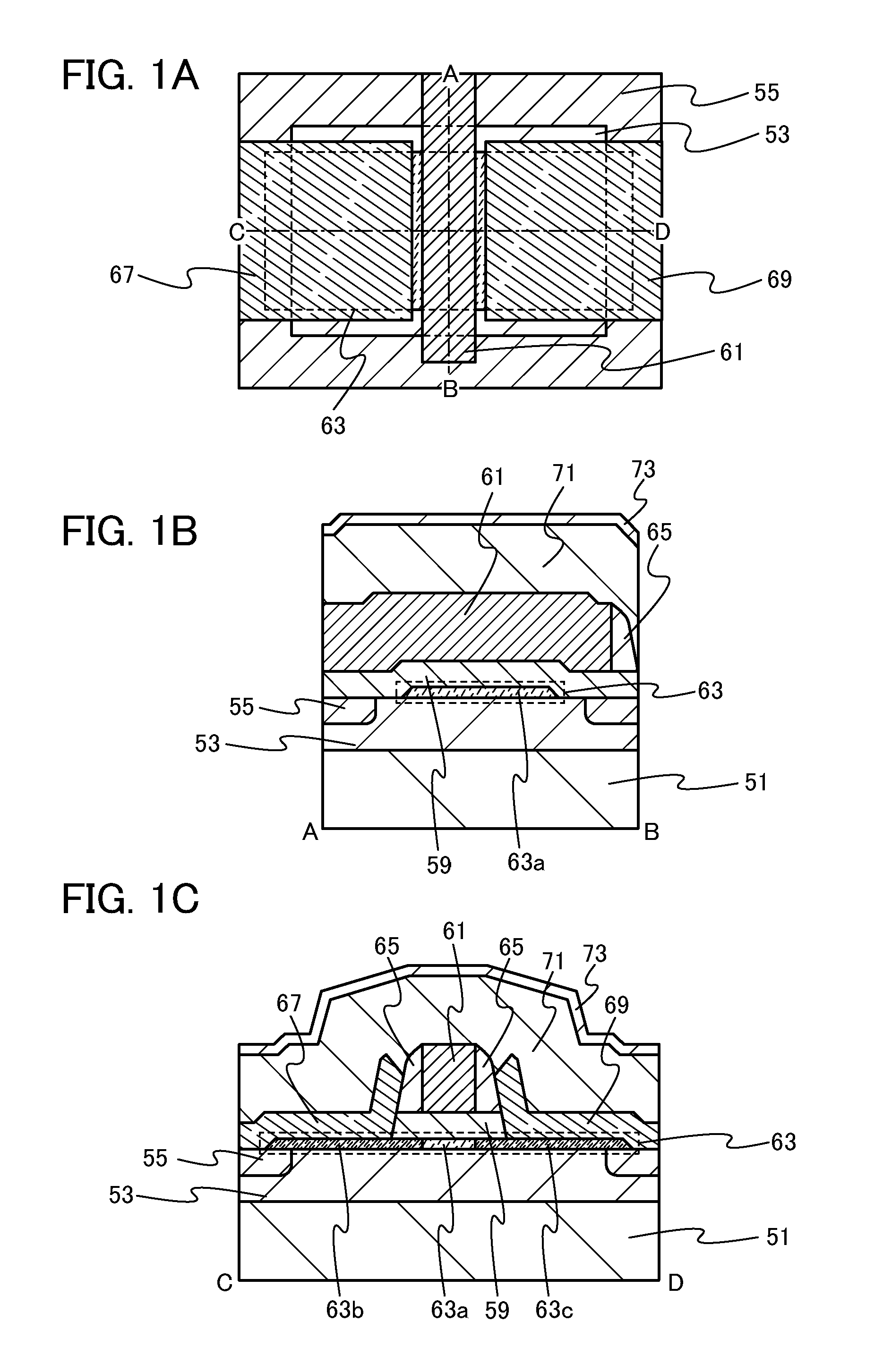
[0036]FIGS. 1A to 1C are a top view and cross-sectional views of a transistor described in this embodiment. FIG. 1A is a top view of the transistor described in this embodiment, FIG. 1B is a cross-sectional view taken along dashed-dotted line A-B in FIG. 1A, and FIG. 1C is a cross-sectional view taken along dashed-dotted line C-D in FIG. 1A. Note that in FIG. 1A, illustration of some components of the transistor (e.g., a gate insulating film 59, sidewall insulating films 65, an insulating film 71, an insulating film 73, and the like) is omitted for simplicity.
[0037]The transistor illustrated in FIGS. 1A to 1C includes a first oxide insulating film 53 over a substrate 51, a second oxide insulating film 55 in the periphery of the first oxide in...
embodiment 2
[0160]In this embodiment, a transistor having a structure different from that of Embodiment 1 and a method for manufacturing the transistor will be described with reference to FIGS. 5A to 5C. In this embodiment, the position of the end portion of the oxide semiconductor film which crosses the channel length direction of the transistor and the position of the boundary between the first oxide insulating film 53 and the second oxide insulating film 55 at the surface in contact with the oxide semiconductor film are different from those in Embodiment 1.
[0161]FIGS. 5A to 5C are a top view and cross-sectional views of a transistor described in this embodiment. FIG. 5A is a top view of the transistor described in this embodiment, FIG. 5B is a cross-sectional view taken along dashed-dotted line A-B in FIG. 5A, and FIG. 5C is a cross-sectional view taken along dashed-dotted line C-D in FIG. 5A. Note that in FIG. 5A, some of components of the transistor (e.g., a gate insulating film 59, sidewa...
embodiment 3
)
[0167]In this embodiment, a transistor having a structure different from those of Embodiments 1 and 2 and a method for manufacturing the transistor will be described with reference to FIGS. 6A and 6B. The transistor in this embodiment includes a pair of wirings in contact with a pair of electrodes, which is a point different from Embodiments 1 and 2. This embodiment will be described as another embodiment of the transistor in Embodiment 2; however, this embodiment can be applied to Embodiment 1 as appropriate.
[0168]FIGS. 6A and 6B are a top view and a cross-sectional view of a transistor described in this embodiment. FIG. 6A is a top view of the transistor described in this embodiment and FIG. 6B is a cross-sectional view taken along dashed-dotted line C-D in FIG. 6A. Note that in FIG. 6A, some of components of the transistor (e.g., a gate insulating film 59, sidewall insulating films 65, an insulating film 71, an insulating film 73, and the like) are omitted for simplicity.
[0169]T...
PUM
 Abstract
Description
Claims
Application Information