Method and system for post-etch treatment of patterned substrate features

a technology of patterned substrates and features, applied in the field of device manufacturing, can solve the problems of disadvantageous roughness or variations due to lwr or ler, process is not without, and the roughness of the patterning substrate is not without, so as to improve the roughness of the set of substrates and improve the patterning. the effect of substrates

Active Publication Date: 2012-10-11
VARIAN SEMICON EQUIP ASSOC INC
View PDF2 Cites 146 Cited by
  • Summary
  • Abstract
  • Description
  • Claims
  • Application Information

AI Technical Summary

Problems solved by technology

Although optical lithography is an efficient process with high throughput, the process is not without disadvantages.
One disadvantage may include line width roughness (LWR) or line edge roughness (LER).
The roughness or variations due to LWR or LER may be disadvantageous as the variation may be transferred onto the trenches during etch and ultimately to the circuit.
Because the geometrical shape of a patterned resist feature, including line roughness effects, such as LWR and LER, is transferred from a resist layer to an underlying permanent layer of a device during patterning of the underlying layer, LWR and LER can limit the ability to form devices of acceptable quality for dimensions below about 100 nm.
Such variations may lead to non-uniform circuits and ultimately device degradation or failure.
In addition, depending on design criteria, device performance may be impacted more by either one of short, medium, or long range roughness.
In one example, dry chemical etch process have the ability to remove resist, but generally suffer from pattern dependent loading effects, in which the removal is different in densely patterned regions as opposed to isolated features.
Such dry chemical etching processes may also impart unwanted defects into a resist pattern, which could result in yield loss.
This creates a challenge to develop improved resist patterning techniques that are robust and stable over different process conditions, such as substrate temperature, post lithography etch conditions, etc.
In addition to the above issues, resist trim processes in which the resist critical dimension (CD) is deliberately reduced, may increase sidewall roughness in resist features.

Method used


Image

  • Method and system for post-etch treatment of patterned substrate features
  • Method and system for post-etch treatment of patterned substrate features
  • Method and system for post-etch treatment of patterned substrate features

Examples


Embodiment Construction

[0024]The present invention will now be described more fully hereinafter with reference to the accompanying drawings, in which preferred embodiments of the invention are shown. This invention, however, may be embodied in many different forms and should not be construed as limited to the embodiments set forth herein. Rather, these embodiments are provided so that this disclosure will be thorough and complete, and will fully convey the scope of the invention to those skilled in the art. In the drawings, like numbers refer to like elements throughout.

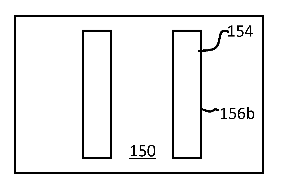
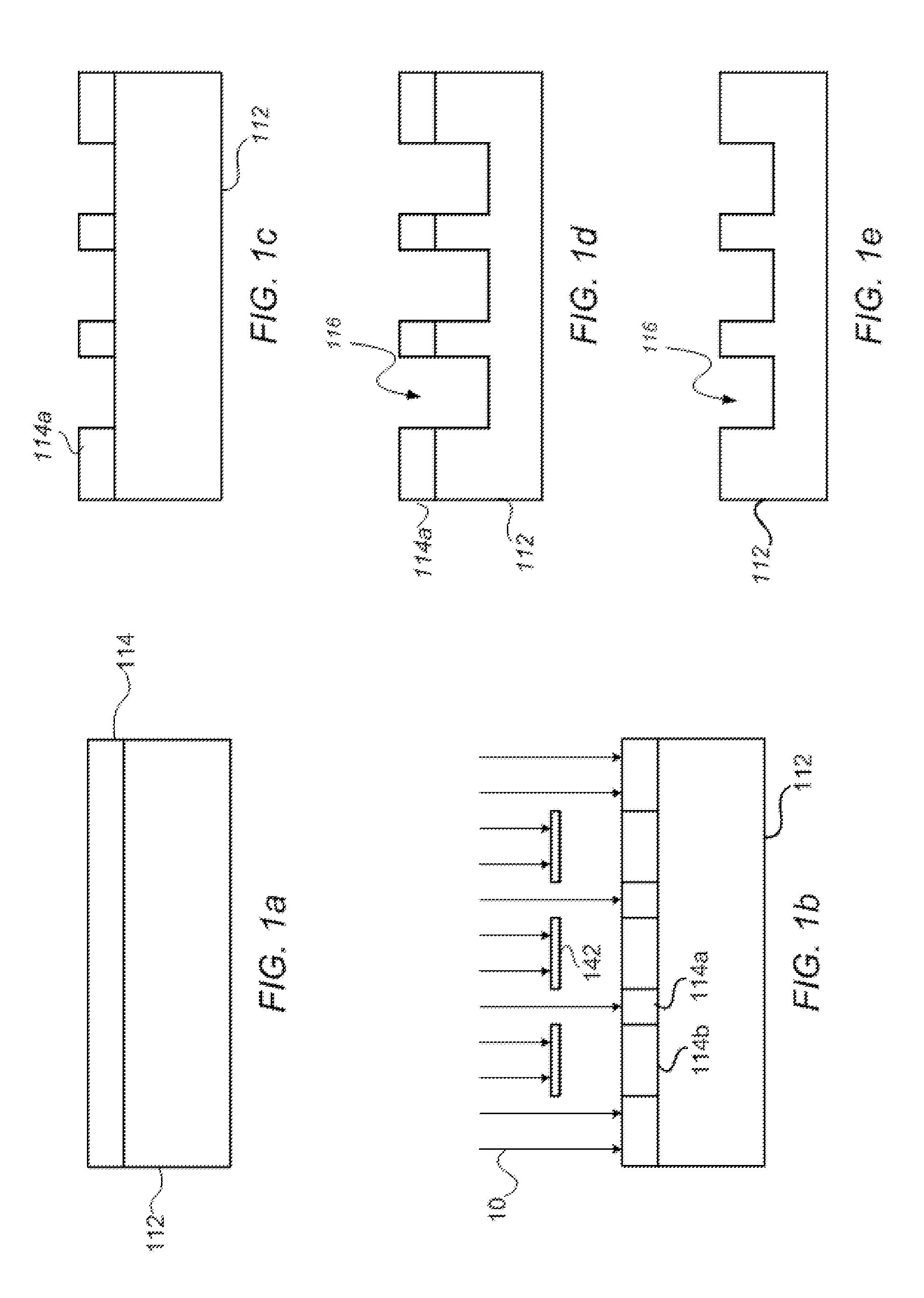
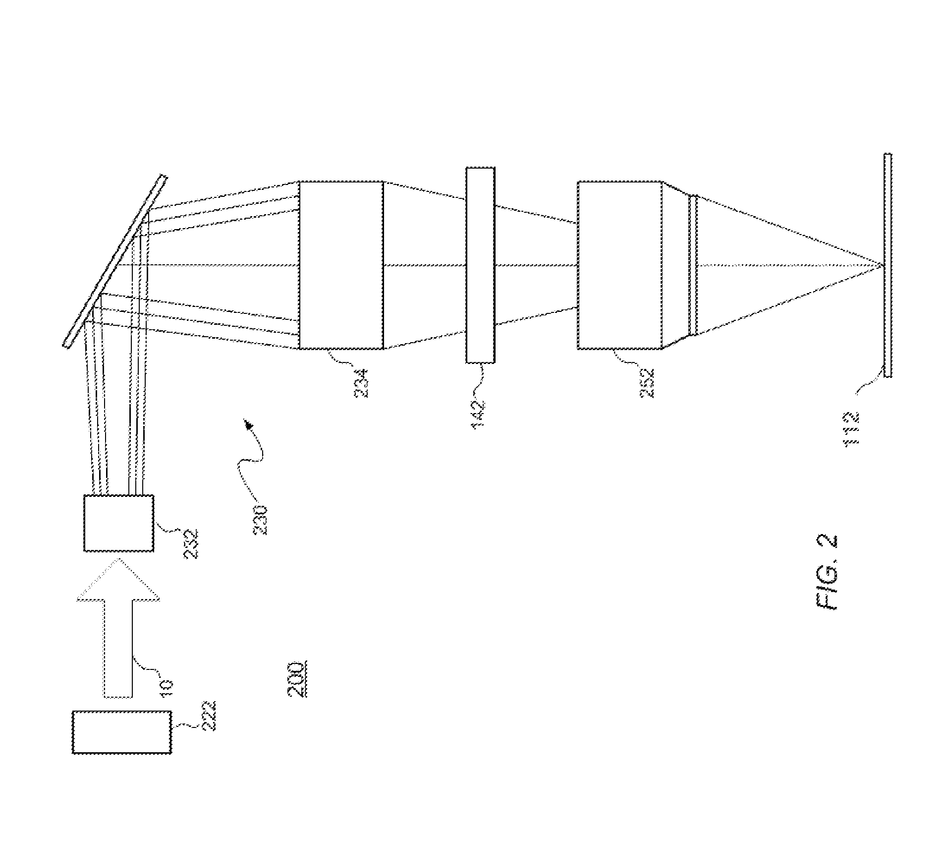
[0025]To solve the deficiencies associated with the methods noted above, novel and inventive techniques and systems for patterning a substrate are introduced. In particular, the present disclosure focuses on techniques involving ion implantation processes for improving the quality of patterning a substrate, such as improving LWR and LER in patterned narrow substrate features. The methods disclosed herein may be used in conjunction with lit...


PUM

PropertyMeasurementUnit
depthaaaaaaaaaa
depthaaaaaaaaaa
angleaaaaaaaaaa

Abstract

A method of patterning a substrate, comprises providing a set of patterned features on the substrate, exposing the set of patterned features to a dose of ions incident on the substrate over multiple angles, and selectively etching exposed portions of the patterned features.

Description

BACKGROUND OF THE INVENTION[0001]1. Field of the Invention[0002]Embodiments relate to the field of device manufacturing. More particularly, the present invention relates to a method, system and structure for patterning a substrate and for implanting into a substrate.[0003]2. Discussion of Related Art[0004]Optical lithography is often used in manufacturing electronic devices. Referring to FIG. 1a-1e, there are shown simplified illustrations of an optical lithographic process. Generally, the substrate 112 is coated with photo-curable, polymeric photoresist 114 (FIG. 1a). Thereafter, a mask 142 having a desired aperture pattern is disposed between the substrate 114 and a light source (not shown). The light 10 from the light source is illuminated onto the substrate 112 via the aperture of the mask 142, and the light transmitted through the mask's aperture (or the image of the pattern) is projected onto the photoresist 114. A portion of the photoresist 114a is exposed to the light 10 and...

Claims


Application Information

Patent Timeline
Patent Type & Authority Applications(United States)
IPC IPC(8): H01L21/306
CPCH01L21/306H01L21/3105H01L21/311H01L21/31155H01L21/3213H01L21/2658H01L21/26586H01L21/321
Inventor GODET, LUDOVICHATEM, CHRISTOPHER R.MARTIN, PATRICK M.MILLER, TIMOTHY J.
Owner VARIAN SEMICON EQUIP ASSOC INC
Why Eureka
Try Eureka