Eureka AIR delivers breakthrough ideas for toughest innovation challenges, trusted by R&D personnel around the world.

Horizontal emitting, vertical emitting, beam shaped, distributed feedback (DFB) lasers fabricated by growth over a patterned substrate with multiple overgrowth

a technology of patterned substrates and lasers, applied in semiconductor lasers, instruments, optical elements, etc., can solve the problems of difficult manufacturing of nitride lasers, difficult cleavage, and difficult vcsels, and achieve the effect of improving the lasing mirror properties

Inactive Publication Date: 2007-06-07
RGT UNIV OF CALIFORNIA
View PDF15 Cites 57 Cited by
  • Summary
  • Abstract
  • Description
  • Claims
  • Application Information

AI Technical Summary

Benefits of technology

[0046] due to a high index difference with the active layer, the patterned layers efficiently confine a laser mode to the active layer;
[0049] the patterned layers isolate the laser mode from one or more electrodes, thus diminishing absorption losses.
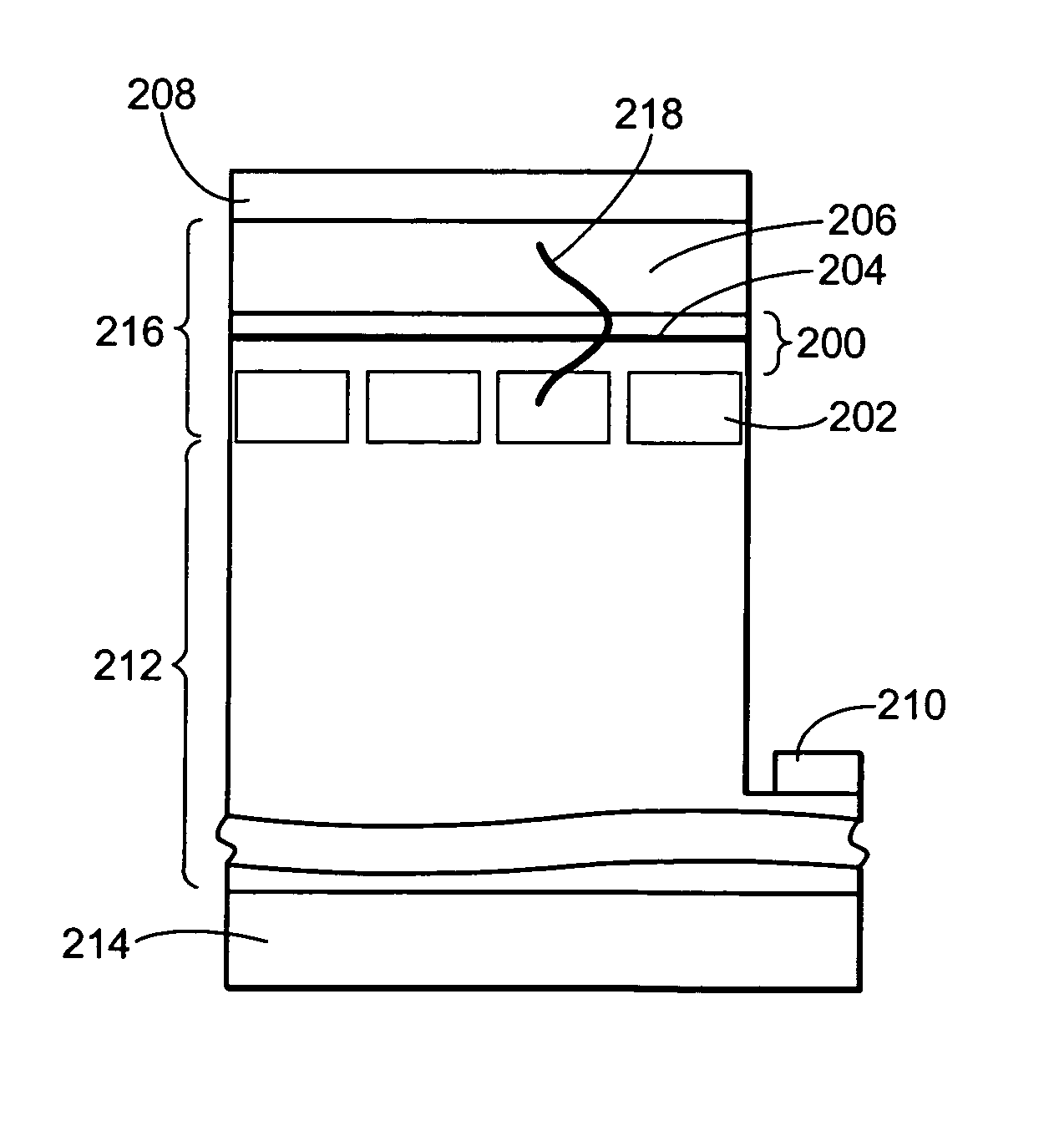
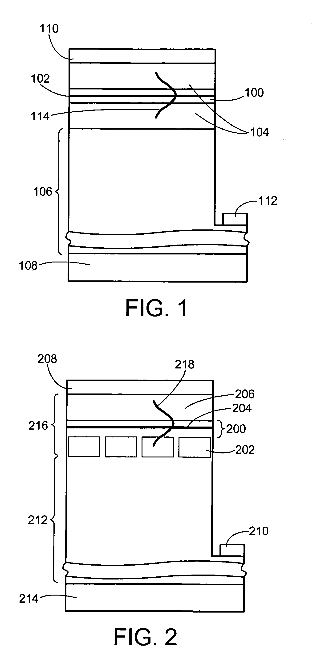
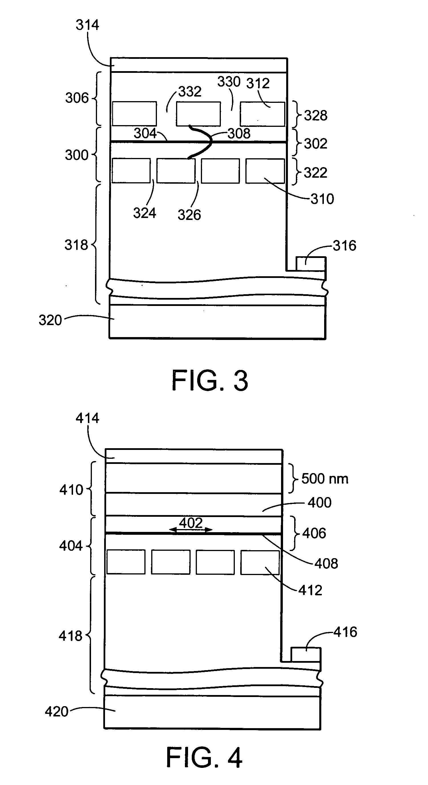
[0051] The first or second patterned layer may have separate gain and two mirror regions. The gain and mirror regions may have different periods, one of the mirrors may comprise an extraction region for extracting or outcoupling. The separate gain, mirror and extraction regions may have different growth depths, defined by etching of the first or second patterned layers, to provide improved mirror properties for lasing in the gain and mirror regions and outcoupling in the extraction region, and wherein a guided mode interacts more strongly with silicon dioxide columns in the mirror regions.

Problems solved by technology

Unfortunately, besides huge materials challenges, nitride lasers are difficult to manufacture.
Moreover, cleavage is hard to achieve because of the sapphire substrate.
VCSELS are, however, extremely hard to obtain, as the high quality mirrors required prove extremely difficult to manufacture, and VCSEL action has not yet been obtained in GaN based lasers.
However, a serious problem arises with the structures described in U.S. Utility application Ser. No. 11 / 067,957, attorneys' docket number 30794.121-US-01 (2005-144-1).
The confining power of the typical materials used to confine light in a nitride materials system, e.g. Aluminum Gallium Nitride (AlGaN), is not strong enough, because the typical materials do not have a high enough refractive index contrast with the active material GaN.
Then, if a thick top confining layer is used to separate the optical wave from the metal electrode, the optical wave will be poorly confined in the active material region, meaning that it will only weakly interact with the pattern of the LEO mask layer.
However such solutions introduce new fabrication steps, and lead to some degree of radiation loss, for instance, at the junction between thinner and thicker confining layers.

Method used


Image

  • Horizontal emitting, vertical emitting, beam shaped, distributed feedback (DFB) lasers fabricated by growth over a patterned substrate with multiple overgrowth
  • Horizontal emitting, vertical emitting, beam shaped, distributed feedback (DFB) lasers fabricated by growth over a patterned substrate with multiple overgrowth
  • Horizontal emitting, vertical emitting, beam shaped, distributed feedback (DFB) lasers fabricated by growth over a patterned substrate with multiple overgrowth

Examples


Embodiment Construction

[0071] In the following description of the preferred embodiment, reference is made to the accompanying drawings that form a part hereof, and in which is shown by way of illustration a specific embodiment in which the invention may be practiced. It is to be understood that other embodiments may be utilized and structural changes may be made without departing from the scope of the present invention.

[0072] Overview

[0073] The present invention relates to improving semiconductor lasers incorporating buried grating mirrors and photonic crystals, and more particularly, to new structures grown on substrates patterned by these gratings and photonic crystals. Specifically, the present invention describes new laser structures with improved contact structures and reduced waveguiding loss by contact electrodes, wherein these laser structures rely on active layers directly grown on patterned substrates with multiple Lateral Epitaxial Overgrowth (LEO).

[0074] Similar to the structures described ...


PUM


Abstract

A structure using integrated optical elements is comprised of a substrate, a buffer layer grown on the substrate, one or more first patterned layers deposited on top of the buffer layer, wherein each of the first patterned layers is comprised of a bottom lateral epitaxial overgrowth (LEO) mask layer and a LEO nitride layer filling holes in the bottom LEO mask layer, one or more active layers formed on the first patterned layers, and one or more second patterned layers deposited on top of the active layer, wherein each of the second patterned layers is comprised of a top LEO mask layer and a LEO nitride layer filling holes in the top LEO mask layer, wherein the top and / or bottom LEO mask layers act as a mirror, optical confinement layer, grating, wavelength selective element, beam shaping element or beam directing element for the active layers.

Description

CROSS-REFERENCE TO RELATED APPLICATIONS [0001] This application claims the benefit under 35 U.S.C Section 119(e) of U.S. Provisional Application Ser. No. 60 / 741,935, filed on Dec. 2, 2005, by Claude C. A. Weisbuch and Shuji Nakamura, entitled “IMPROVED HORIZONTAL EMITTING, VERTICAL EMITTING, BEAM SHAPED, DISTRIBUTED FEEDBACK (DFB) LASERS FABRICATED BY GROWTH OVER A PATTERNED SUBSTRATE WITH MULTIPLE OVERGROWTH,” attorneys' docket number 30794.143-US-P1 (2005-721); [0002] which application is incorporated by reference herein. [0003] This application is related to the following co-pending and commonly-assigned applications: [0004] U.S. Utility application Ser. No. 10 / 581,940, filed on Jun. 7, 2006, by Tetsuo Fujii, Yan Gao, Evelyn. L. Hu, and Shuji Nakamura, entitled “HIGHLY EFFICIENT GALLIUM NITRIDE BASED LIGHT EMITTING DIODES VIA SURFACE ROUGHENING”, attorney's docket number 30794.108-US-WO (2004-063), which application claims the benefit under 35 U.S.C Section 365(c) of PCT Applicat...

Claims


Application Information

Patent Timeline
IPC IPC(8): H01L29/06H01L27/15H01S5/12H01S5/18
CPCB82Y20/00H01S2304/12H01L21/02647H01L33/007H01S5/105H01S5/12H01S5/1206H01S5/1215H01S5/1225H01S5/1231H01S5/18H01S5/187H01S5/20H01S5/2004H01S5/34333G02B6/1225H01S5/11
Inventor WEISBUCH, CLAUDE C.A.NAKAMURA, SHUJI
Owner RGT UNIV OF CALIFORNIA
Why Eureka
Eureka Blog
Learn More