

Temperature-measuring substrate and heat treatment apparatus
- Summary
- Abstract
- Description
- Claims
- Application Information
AI Technical Summary
Benefits of technology
Problems solved by technology
Method used
Image

Examples
first embodiment
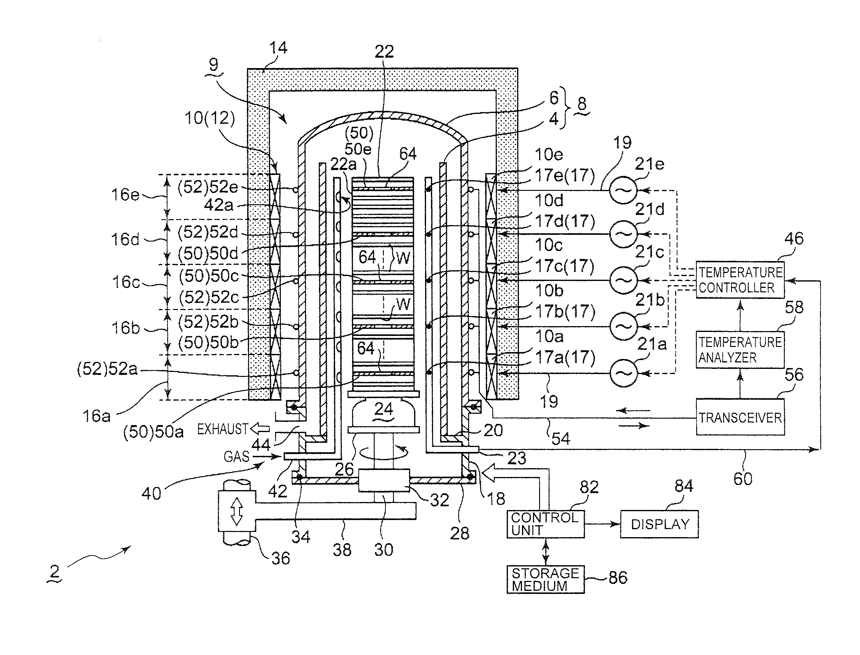
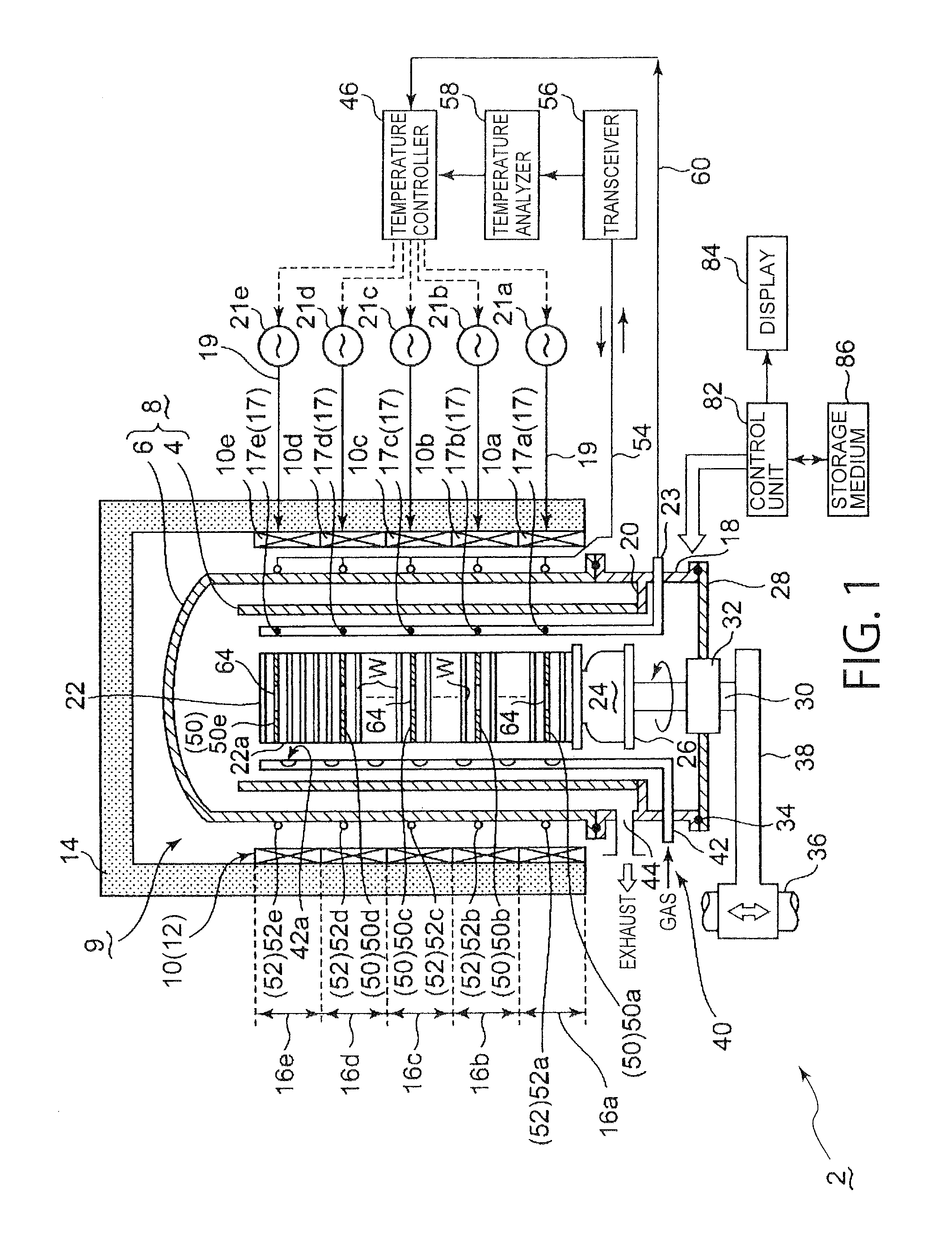
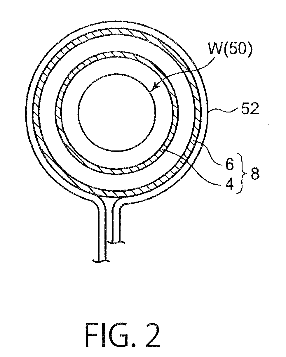
[0047]The temperature-measuring substrates 50 (50a to 50e) will now be described in detail. As shown in FIGS. 4A and 4B, the temperature-measuring substrate 50 is mainly comprised of a disk-shaped substrate body 62, an oscillator provided in the substrate body 62, and an antenna portion 66 provided around the substrate body 62. The oscillator 64 includes a piezoelectric element 68 having the shape of a thin plate, and a pair of electrodes 70 (see FIG. 5) bonded to both sides of the piezoelectric element 68. The entire piezoelectric element 68 is housed in an airtight case 72 e.g. made of an insulating material or a semiconducting material, and the case 72 is embedded in the substrate body 62.
[0048]Alternatively, the substrate body 62 may be composed of two thin substrates bonded together, with the oscillator 64 being confined between the substrates. When the two thin substrates are formed of the same material as a semiconductor wafer, such as silicon, there is no need to use the ca...
second embodiment
[0074]In the temperature-measuring substrate 50 shown in FIGS. 4A and 4B, the circular ring-shaped antenna installation portion 74 is provided around the substrate body 62. In the second embodiment shown in FIG. 8(A), on the other hand, a peripheral portion of a disk-shaped substrate body 62 is cut in a line, and an antenna installation portion 74 of insulating material, having the same shape as the cutout portion, is bonded to the cut site of the substrate body 62, e.g. by fusion bonding. An antenna portion 66, comprised of a coiled antenna wire 76, is formed in the antenna installation portion 74.
[0075]In this embodiment the diameter and the thickness of the substrate body 62 are set equal to those of semiconductor wafers W to be processed in order to avoid any trouble in carrying the substrate or a wafer into and out of the wafer boat 22. The temperature-measuring substrate of this embodiment can achieve the same advantageous effects as the temperature-measuring substrate of the ...
third embodiment
[0078]The temperature-measuring substrate 50 of this embodiment can achieve the same advantageous effects as the temperature-measuring substrate of the preceding embodiment shown in FIGS. 4A and 4B. Furthermore, because the antenna installation portion 74 projects laterally radio waves can be prevented from being adversely affected by silicon substrates, lying above and below the temperature-measuring substrate 50, during heat treatment.
[0079]
[0080]Temperature-measuring substrates according to fourth to eighth embodiments of the present invention will now be described. Though in the above-described temperature-measuring substrates 50 according to the first to third embodiments, one oscillator 64 and one antenna portion 66 are provided for one temperature-measuring substrate 50, it is also possible to provide a plurality of oscillators and antenna portions connected to the oscillators for one temperature-measuring substrate 50.
[0081]FIGS. 9A to 9D are plan views showing such tempera...
PUM
 Abstract
Description
Claims
Application Information