

Low-Voltage-Driven Boost Circuit and Associated Method
- Summary
- Abstract
- Description
- Claims
- Application Information
AI Technical Summary
Benefits of technology
Problems solved by technology
Method used
Image

Examples
Embodiment Construction
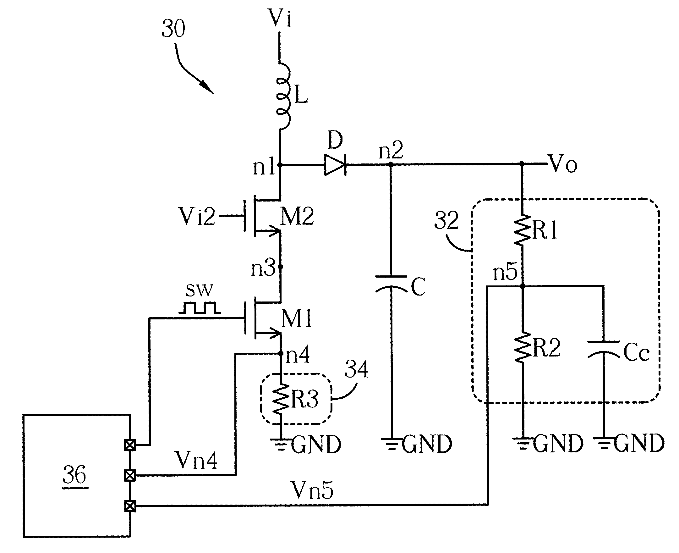
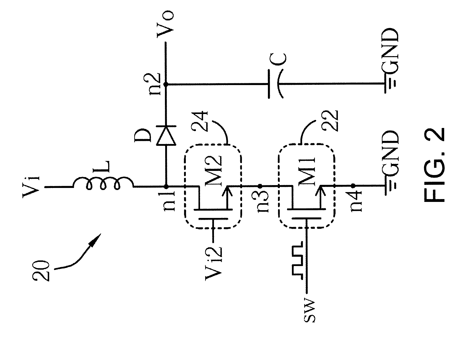
[0022]FIG. 2 shows a schematic diagram of a boost circuit 20 according to an embodiment of the present invention. The boost circuit 20 draws a voltage Vi and provides an output voltage Vo at a node n2. The boost circuit 20 comprises an inductor L, a diode D, a capacitor C, and two switches 22 and 24.
[0023]In the boost circuit 20, the inductor L is coupled between the voltage Vi and a node n1. The diode may be a Schottky diode, and has its anode and cathode respectively coupled to the nodes n1 and n2. The capacitor C is coupled between the node n2 and a ground voltage GND. The switch 22 may be realized by a transistor M1. For example, the transistor M1 is an n-channel metal oxide semiconductor (NMOS), which has drain, source and gate serving as two channel ends and a control end of the switch 22 respectively. The two channel ends and the control end of the switch 22 are respectively coupled to nodes n3, n4 and a switch circuit sw, so as to selectively conduct the switch 22 between th...
PUM
 Abstract
Description
Claims
Application Information