Charged particle beam microscope and method of measurement employing same

a charge particle and microscope technology, applied in the field of charge particle beam microscope and charge particle beam microscopy, can solve the problems of specimen drift, blurring and distortion in formed images, and stored images with blurring in the drift direction, and achieve the effect of reducing the effect of specimen drift on images

Active Publication Date: 2012-11-15
HITACHI HIGH-TECH CORP
View PDF1 Cites 29 Cited by
  • Summary
  • Abstract
  • Description
  • Claims
  • Application Information

AI Technical Summary

Benefits of technology

[0023]The present invention can provide an electric charged particle beam microscope and electric charged particle beam microscopy capable of reducing the effect of specimen drift on images even for high-resolution, high-SNR imaging.

Problems solved by technology

Specimen drift may cause blurring and distortion in formed images.
The integrated image shifts result in a stored image having blurring in the drift direction.
On the other hand, the specimen drift occurring during the slow-scan mode operation causes image distortion in the drift direction (FIG. 2C).

Method used


Image

  • Charged particle beam microscope and method of measurement employing same
  • Charged particle beam microscope and method of measurement employing same
  • Charged particle beam microscope and method of measurement employing same

Examples


embodiment 1

[0041]Embodiment 1 shows a STEM to which a system for automatically compensating for image distortion caused by specimen drift is applied.

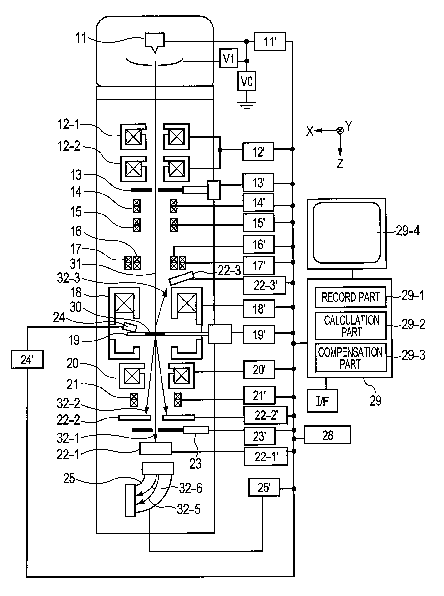
[0042]FIG. 7 shows a basic configuration of the STEM / SEM used in Embodiment 1. A direction substantially parallel to the optical axis of the optical column is assumed to be the Z direction and a plane substantially orthogonal to the optical axis is assumed to be the XY plane. The STEM / SEM system includes an electron gun 11, which is an electric charged particle source, for emitting a primary electron beam 31, an electron gun control unit 11′, condenser lenses 12-1, 12-2 for converging the primary electron beam 31 emitted from the electron gun, a condenser lens control unit 12′, a condenser aperture 13 for controlling the divergent angle of the primary electron beam 31, a condenser aperture control unit 13′, an alignment deflector 14 for controlling the incidence angle of the beam to a specimen 30, an alignment deflector control unit 14′, a stigmat...

embodiment 2

[0055]In Embodiment 2, as with the case of Embodiment 1, the apparatus shown in FIG. 7 measures specimen drift before forming images, forms an image while compensating for the specimen drift by an image shift deflector 16, and executes distortion compensation after forming the image through the image processing described in Embodiment 1. The matters that are described in Embodiment 1, but not in Embodiment 2, should be considered as being included in Embodiment 2.

[0056]FIG. 8 shows a flow of compensating for specimen drift in Embodiment 2. Steps (S5) for compensating for specimen drift by an image shift deflector during imaging are added to the basic flow shown in FIG. 3.

[0057]First, specimen drift is measured by using fast-scan images (S5-1), and an approximation function of the specimen drift occurred during imaging is determined (S5-2). In Embodiment 2, the number of images to be captured is set to 3 or more, and the approximation function of the specimen drift is obtained from t...

embodiment 3

[0060]Embodiment 3 shows an example in which the present invention is applied to an apparatus capable of providing multiple types of electric charged particle beams. The matters that are described in Embodiments 1 and 2, but not in Embodiment 3, should be considered as being included in Embodiment 3.

[0061]As with the case of Embodiments 1 and 2, Embodiment 3 also uses the same apparatus as shown in FIG. 7. The apparatus in FIG. 7 is equipped with a plurality of detectors: a detector 22-3 for detecting secondary electrons emitted backward from the specimen 30; an electron detector for bright-field images 22-1 for detecting low angle scattering electrons out of electron beams emitted forward from the specimen 30; and an electron detector for dark-field images 22-2 for detecting high angle scattering electrons out of electron beams emitted forward from the specimen 30. In addition, a transmitted electron beam can be split into elastically scattered electron beam 32-5 and inelastically ...


PUM


Abstract

The electric charged particle beam microscope includes an electric charged particle source; a condenser lens converging electric charged particles emitted from the electric charged particle source on a specimen; a deflector scanning the converged electric charged particles over the specimen; a control unit of the deflector; a specimen stage on which the specimen is mounted; a detector detecting the electric charged particles; a computer forming an image from a control signal from the deflector and an output signal from the detector; and a display part connected with the computer. The control unit of the deflector can change the scan rate of the electric charged particles. A first rate scan image is obtained at a first rate and a second rate scan image is obtained at a second rate slower than the first rate.

Description

TECHNICAL FIELD[0001]The present invention relates to an electric charged particle beam microscope and electric charged particle beam microscopy.BACKGROUND ART[0002]In semiconductor device development and nano-material development, electric charged particle beam microscopes and electric charged particle beam microscopy capable of analyzing specimen structure at a spatial resolution power of an order of nanometer (nm) are essential. The electric charged particle beam microscopes are categorized into various types according to the beams to be used. One of these microscopes is a scanning transmission electron microscope (STEM) that scans over a specimen with a converged narrow electron beam and detects electron beams that have been transmitted through the specimen to form an image, and another is a scanning electron microscope (SEM) that detects secondary electrons and backscattered electrons to form an image. Ion microscopes using ions as incident beams are also a type of electric cha...

Claims


Application Information

Patent Timeline
Patent Type & Authority Applications(United States)
IPC IPC(8): H04N7/18
CPCH01J37/265H01J2237/2809H01J2237/221H01J37/28
Inventor TSUNETA, RURIKOKIKUCHI, HIDEKI
Owner HITACHI HIGH-TECH CORP
Why Eureka
Try Eureka