Microelectromechanical device and system
- Summary
- Abstract
- Description
- Claims
- Application Information
AI Technical Summary
Benefits of technology
Problems solved by technology
Method used
Image

Examples
Embodiment Construction
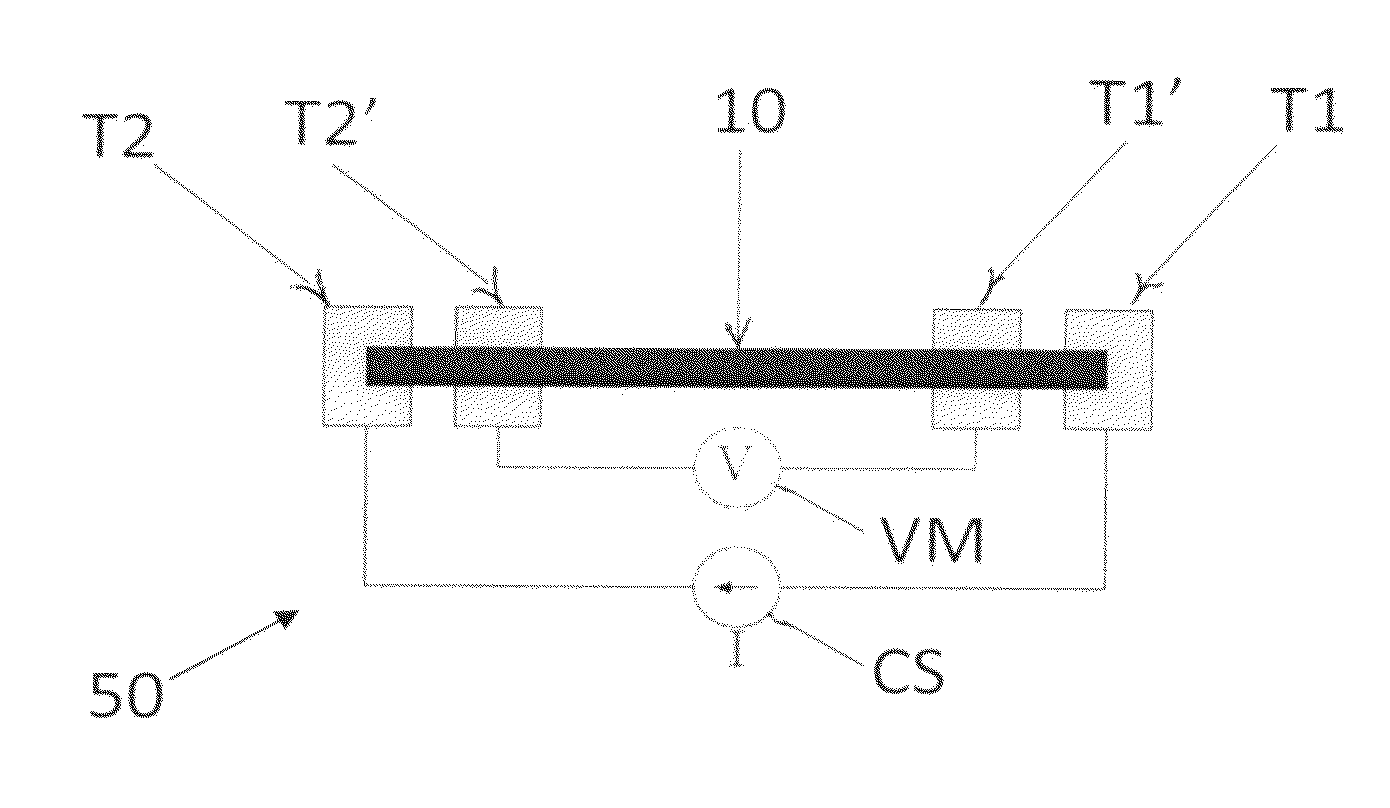
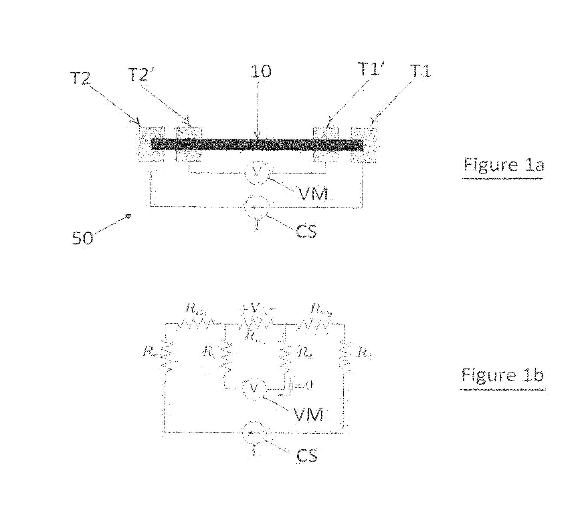
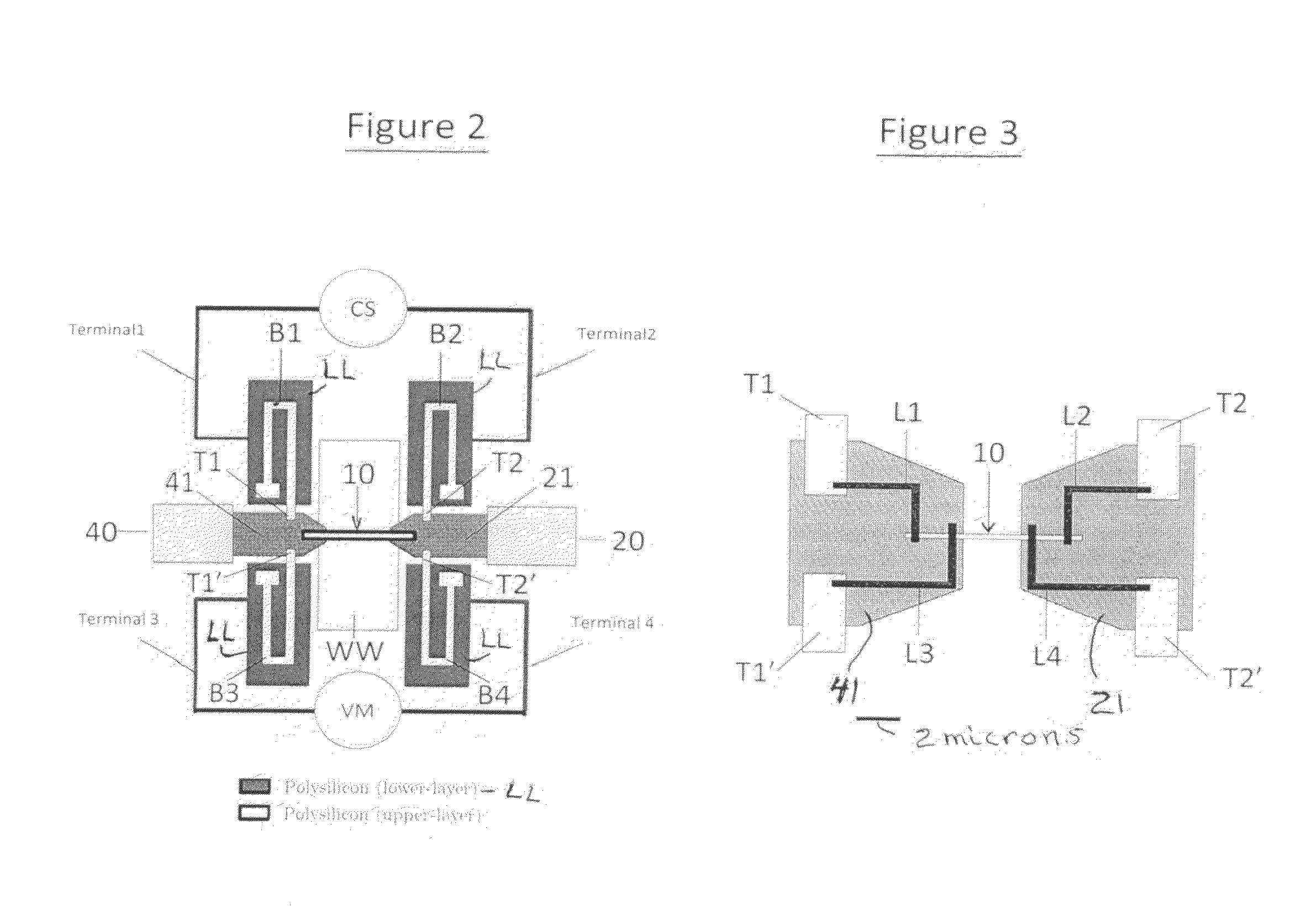
[0022]The present invention described herein provides a microelectromechanical device (MEMD) fabricated by surface micromachining on a multi-layered semiconductor substrate (e.g. silicon substrate or chip) for electrical and mechanical characterization (testing) of a specimen having a nano-scale dimension. The device can be used to test a nanostructure such as carbon nanotube (CNT), nanowire (NW) and nanoscale thin film such as a graphene layer having a nano-scale dimension, which is 200 nm or less (such as specimens having a dimension from 100-200 nm can be tested). For example, for a CNT, the nano-scale dimension can be the CNT diameter and / or the CNT length. For a NW, the nano-scale dimension can be the NW diameter and / or the NW length. For a thin film, the nano-scale dimension typically is the film thickness which is less than 100 nm.
[0023]Pursuant to the present invention, the microelectromechanical device (MEMD) incorporates four-terminal Kelvin electrical characterization (sp...
PUM
 Abstract
Description
Claims
Application Information