Graphene nanomesh and method of making the same

a graphene nanomeh and nanomeh technology, applied in the field of graphene, can solve the problems of not being able to obtain gnrs in the sub 10 nm regime experimentally, preventing this method from being used to obtain gnrs with a sufficiently large band gap for room temperature fets, etc., to achieve uniform periodicity and uniform neck width

Inactive Publication Date: 2012-11-29
RGT UNIV OF CALIFORNIA
View PDF4 Cites 45 Cited by
  • Summary
  • Abstract
  • Description
  • Claims
  • Application Information

AI Technical Summary

Benefits of technology

[0009]In one embodiment of the invention, a graphene nanomesh includes a sheet of graphene having a plurality of periodically arranged apertures, wherein the plurality of apertures have a substantially uniform periodicity and substantially uniform neck width. The periodicity of apertures may vary depending the particular application a

Problems solved by technology

However, two-dimensional graphene is a semi-metal with zero band gap and remains highly conductive even at the charge neutrality point, and therefore, cannot be used for field-effect transistors (FETs) at room temperature.
However, it is non-trivial to obtain GNRs in the sub 10 nm regime experimentally.
However, the smallest GNR width that can be obtained using e-beam lithography is about 15-20 nm, which prevents this method from being used to obtain GNRs with a sufficiently large band gap for room temperature FETs.
Additionally, GNRs fabricated by e-beam lithography usually have a line edge roughness of 1-3 nm, which can adversely impact their electronic properties, and makes it practically impossible to obtain uniform GNRs in the sub 5 nm regime using conventional lithography.
However, the GNRs obtained with this method came from

Method used


Image

  • Graphene nanomesh and method of making the same
  • Graphene nanomesh and method of making the same
  • Graphene nanomesh and method of making the same

Examples


Embodiment Construction

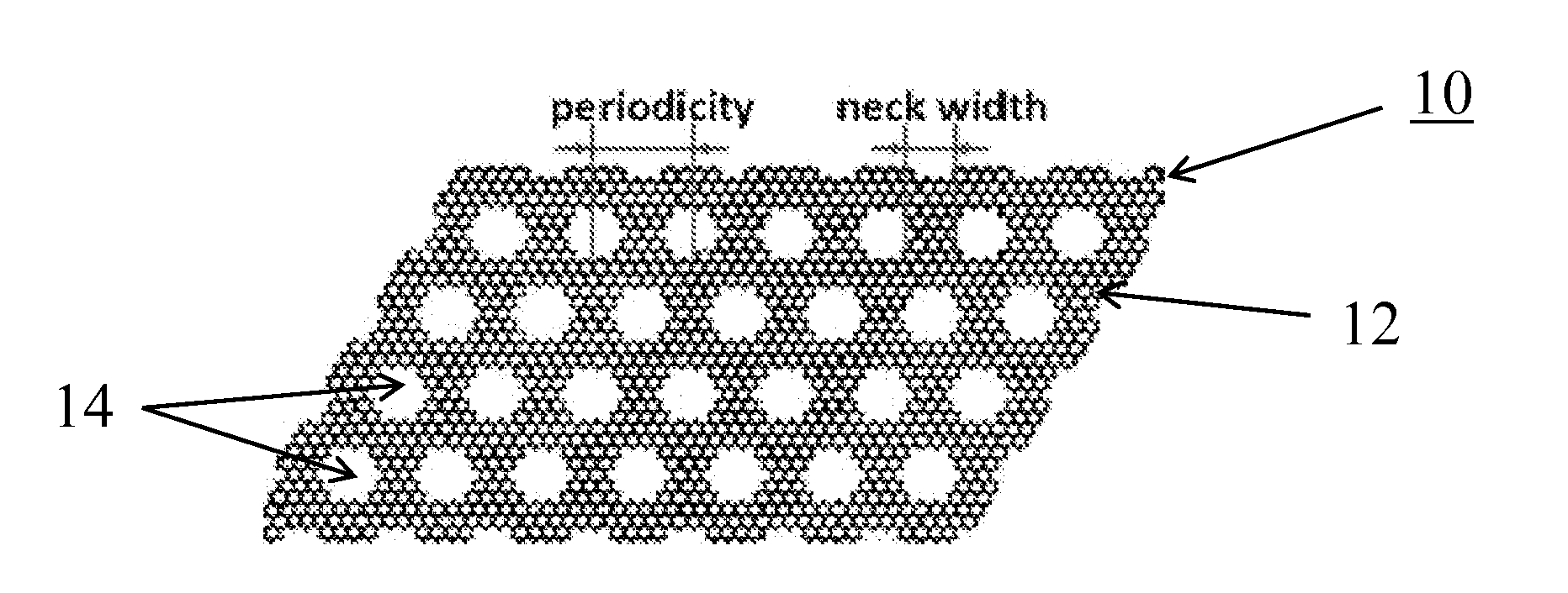
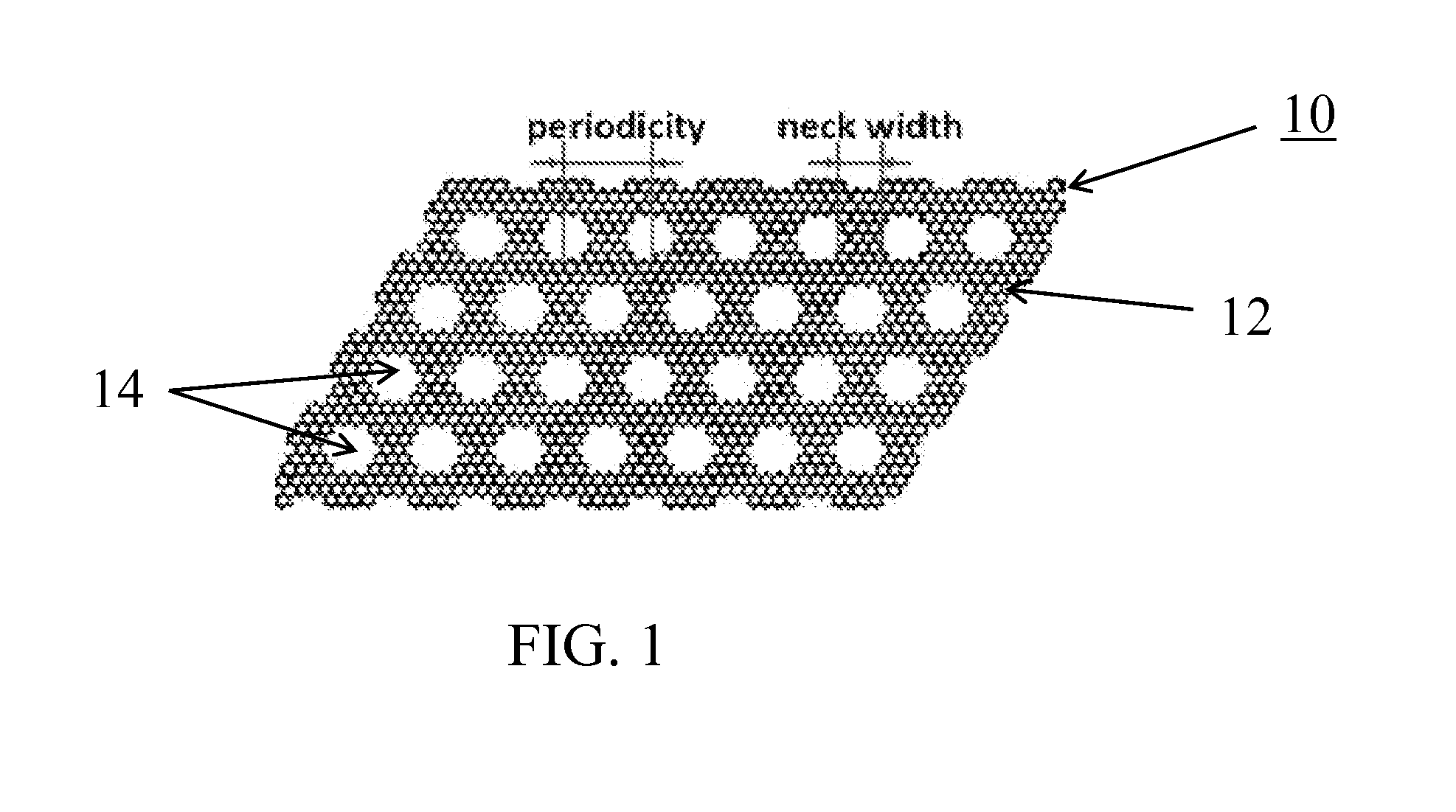
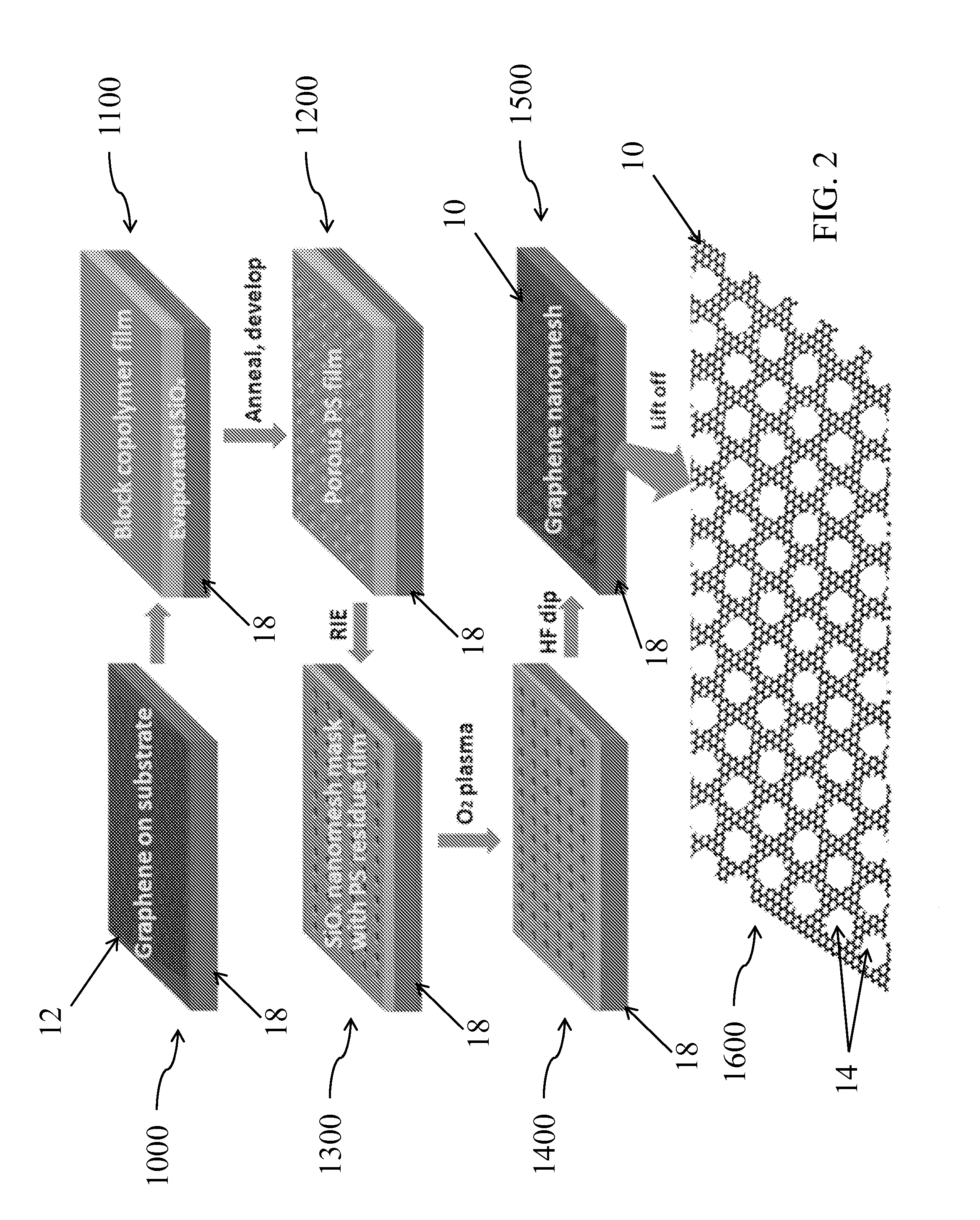
[0041]FIG. 1 illustrates a schematic illustration of graphene nanomesh 10. The graphene nanomesh 10 includes a sheet 12 of graphene having a plurality of apertures 14 formed therein. The sheet 12 of graphene may have a single layer of graphene or, alternatively, several layers of graphene. The plurality of apertures 14 are periodically arranged throughout the sheet 12. The graphene nanomesh 10 has two structural parameters that affect the electrical properties of the sheet 12. The first structural parameter is the “periodicity” of the apertures 14 and is defined as the center-to-center distance between two neighboring apertures 14. The second structural parameter is the “neck width” of the apertures 14 and is defined as the smallest edge-to-edge distance between two neighboring apertures 14 in the graphene nanomesh 10. Both the periodicity and the neck width are illustrated in FIG. 1.

[0042]Periodicity and neck width define the basic structural information in the graphene nanomesh 10...


PUM


Abstract

A graphene nanomesh includes a sheet of graphene having a plurality of periodically arranged apertures, wherein the plurality of apertures have a substantially uniform periodicity and substantially uniform neck width. The graphene nanomesh can open up a large band gap in a sheet of graphene to create a semiconducting thin film. The periodicity and neck width of the apertures formed in the graphene nanomesh may be tuned to alter the electrical properties of the graphene nanomesh. The graphene nanomesh is prepared with block copolymer lithography. Graphene nanomesh field-effect transistors (FETs) can support currents nearly 100 times greater than individual graphene nanoribbon devices and the on-off ratio, which is comparable with values achieved in nanoribbon devices, can be tuned by varying the neck width. The graphene nanomesh may also be incorporated into FET-type sensor devices.

Description

RELATED APPLICATION[0001]This Application claims priority to U.S. Provisional Patent Application No. 61 / 300,398 filed on Feb. 1, 2010. U.S. Patent Application No. 61 / 300,398 is incorporated by reference as if set forth fully herein. Priority is claimed pursuant to 35 U.S.C. §119 and any other applicable statute.STATEMENT REGARDING FEDERALLY SPONSORED RESEARCH AND DEVELOPMENT[0002]This invention was made with Government support under Grant No. OD004342, awarded by the National Institutes of Health. The Government has certain rights in this inventionFIELD OF THE INVENTION[0003]The field of the invention generally relates graphene and, in particular, methods of making graphene nanomesh and devices incorporating graphene nanomesh.BACKGROUND OF THE INVENTION[0004]Graphene is the two-dimensional crystalline form of carbon made of a single layer of carbon atoms arranged in hexagons, like a honeycomb. Graphene has attracted considerable interest as a new electronic material for fundamental ...

Claims


Application Information

Patent Timeline
IPC IPC(8): H01B1/04C12M1/40C01B31/00H01L29/08H01L21/3065B32B3/24B32B3/30G01N27/00H01L21/308B82Y30/00
CPCB82Y30/00B82Y40/00C01B31/0484H01L29/66742H01L29/78684Y10T428/24273G01N27/4145G01N27/4146Y10T428/24331Y10T428/24479H01L29/78696C01B32/194
Inventor DUAN, XIANGFENGHUANG, YUBAI, JINGWEI
Owner RGT UNIV OF CALIFORNIA
Why Eureka
Try Eureka