Method of Joining Metal-Ceramic Substrates to Metal Bodies

a metal-ceramic substrate and metal body technology, applied in gaseous cathodes, electric discharge lamps, electrical apparatus, etc., can solve the problems of reducing heat transfer, failure of components, and unsuitable for fastening, and achieve stronger and more stable bonding of metal bodies, better long-term properties, and better property profiles

Active Publication Date: 2012-12-06
IXYS SEMICON
View PDF7 Cites 16 Cited by
  • Summary
  • Abstract
  • Description
  • Claims
  • Application Information

AI Technical Summary

Benefits of technology

[0019]Herein a method of joining a metal-ceramic substrate to a metal body by means of a metal alloy, where the metal-ceramic substrate has metallization on at least one side, is described. In the process a metal body having a thickness of less than 1 mm is used. A metal alloy which contains aluminium and has a liquidus temperature of greater than 450° C. is arranged between the metal-ceramic substrate and the metal body. The resulting assembly is heated to a temperature of greater than 450° C. Surprisingly this approach makes it possible to provide metal-ceramic modules having a better property profile. The method of the invention allows bonding of metal bodies to ceramic substrates and in particular makes it possible to achieve stronger and more stable bonding of metal bodies to ceramic substrates, with the join also withstanding cyclic thermal stress very well. The formation of cracks and delamination at the join in the case of such cyclic thermal stresses is avoided and better long-term properties, in particular a better long-term heat transfer, of the metal-ceramic modules are thus ensured and the risk of failure of the metal-ceramic module during use is comparatively low. As a result using metal bodies of less than 1 mm thick, only small mechanical stresses which are not critical for the metal-ceramic substrate are generated in the case of thermal stressing of the composite of metal-ceramic substrate and metal body. Thus limitation of the yield stress of the metal bodies to be used is not necessary. The use of further joining means, in particular screws, clamps or other coupling media such as thermal interface materials (TIM) is not required for the purposes of the present invention. Furthermore, the solution according to the invention can be realized inexpensively and efficiently in a comparatively simple way.

Problems solved by technology

Adhesive bonding of ceramic substrates and baseplates, which typically comprise copper (Cu), by means of soft solder with cyclic thermal stressing of the power modules, however, leads to formation of cracks and delamination in the solder layer, which can reduce heat transfer and lead to failure of the component.
This procedure, however, is not suitable for fastening ceramic substrates which have metallization on at least one side to metal bodies utilized for removal of heat since cyclic thermal stress of the power modules leads to formation of cracks and delaminations which can firstly reduce heat transfer and also lead to failure of the component.
Furthermore, this procedure is, particularly as a result of the comparatively high temperatures, complicated and costly.
The methods of these documents in the form in which they are disclosed are, however, in particular because of the single part processing and as a result of the comparatively high temperatures, extremely complicated and costly.
The restriction of the thickness and the yield stress of the baseplates used, as described in EP 2 214 202 A2, also results in a limitation of the possible fields of application.
The low-temperature sintering technology, which has in recent years been successfully used, in particular, for the die-attach method, however, has only limited suitability for joining ceramic substrates to metal bodies since in this process pressures in the range from 2 MPa to 20 MPa have to be employed for producing the sintered join.
Direct cooling of the ceramic substrates by means of the cooling medium in the module construction (e.g. Danfoss ShowerPower®), however, is limited by the maximum possible pressure of the cooling medium due to the risk of intrusion of cooling medium into the component increases with increasing pressure.
Furthermore, the substrate undersides which are in direct contact with the cooling medium can be enlarged only to a limited extent in terms of their surface area, so that in this case there is no optimized contact between ceramic substrate and cooling medium, which in turn has an adverse effect on heat transfer.
This likewise requires one of the known joining technologies for joining ceramic substrate and bottom, e.g. soldering or sintering, with the above-described disadvantages and also can be implemented only for modules having very demanding requirements in terms of reliability, e.g. spaceflight, because of the high costs of material for the baseplates.

Method used


Image

  • Method of Joining Metal-Ceramic Substrates to Metal Bodies
  • Method of Joining Metal-Ceramic Substrates to Metal Bodies

Examples


example 1

Joining of DAB Substrates Metallized on Both Sides and Structured on One Side to an Al—Si-Coated Aluminium Sheet

[0095]In this example, DAB ceramic substrates having a lateral size of 36 mm×20 mm (Al2O3 ceramic (thickness 0.38 mm) with Al metallization (thickness 0.3 mm) on both sides, where the upper side of the DAB substrate is structured for a circuit) are joined to a 0.2 mm thick aluminium sheet coated on one side with Al—Si.

[0096]For the joining process, the substrates to be joined are placed with the unstructured side on the Al—Si-coated side of the aluminium sheet in defined positions.

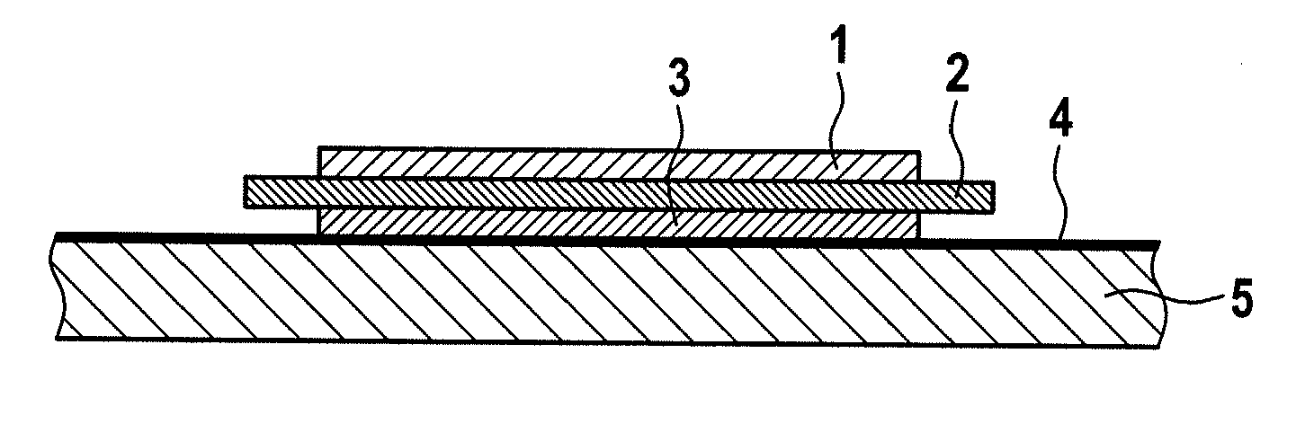
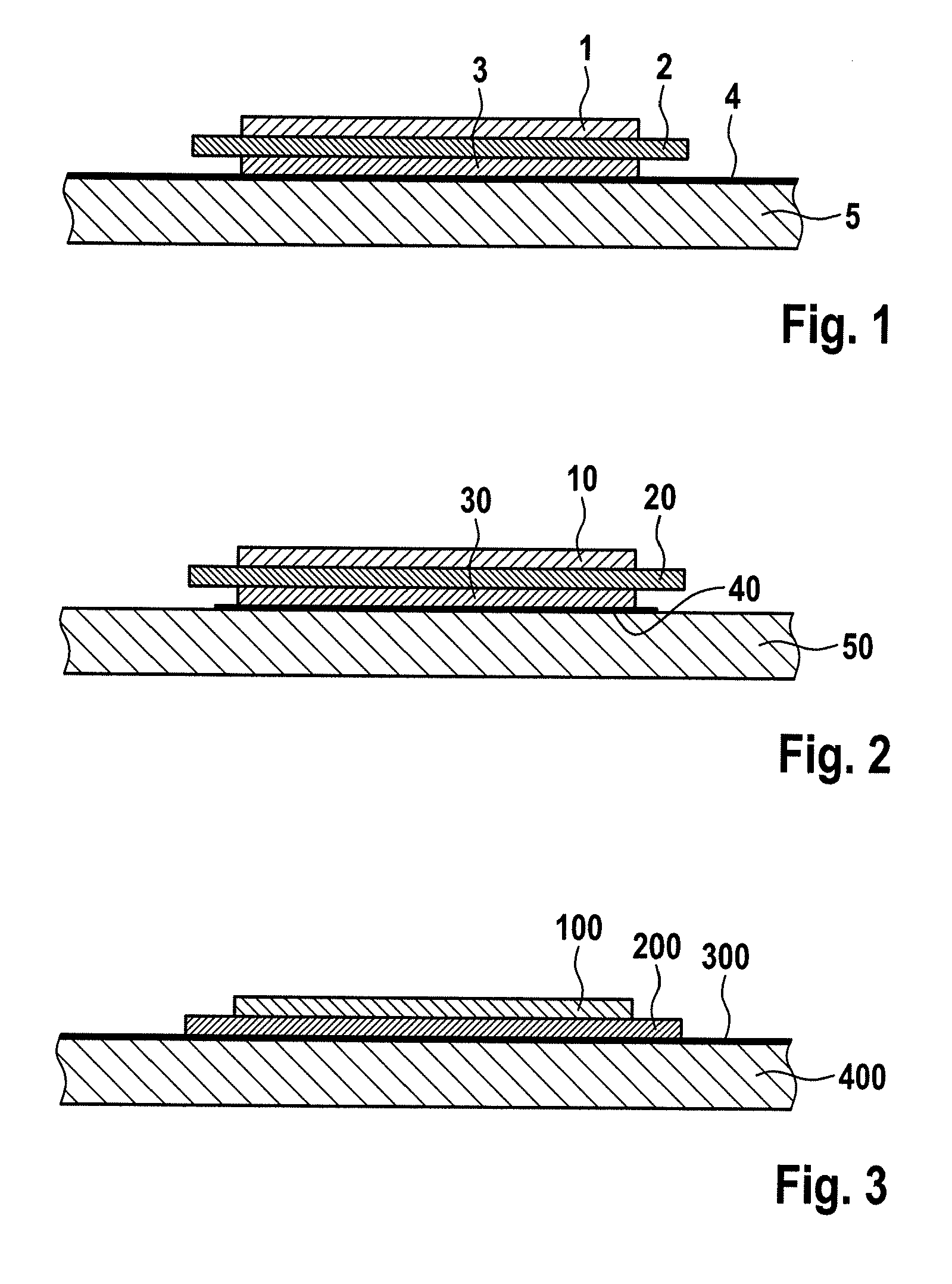
[0097]An in-principle sketch through the cross section of the structure is shown in FIG. 1, where the metallized ceramic substrate comprises a ceramic 2 and metallization 1 and 3 on both sides and the joining layer 4 is firmly joined to the aluminium sheet 5.

[0098]This stack is placed on the conveyor belt of a tunnel kiln having a plurality of heating zones and is moved at a constant transport sp...

example 2

Joining of a Structured DAB Substrate to an Aluminium Sheet by Means of Loosely Laid Al—Si Plates

[0100]In this example, a DAB ceramic substrate having a lateral size of 36 mm×20 mm (Al2O3 ceramic (thickness 0.38 mm) with Al metallization (thickness 0.3 mm) on both sides) is joined to a 0.8 mm thick Al sheet, with the upper metallization of the DAB substrate being structured for a circuit. Before the joining process, an Al—Si plate having a size of 36 mm×20 mm and a thickness of 0.075 mm for each substrate to be joined is placed in the defined positions on the upper side of the aluminium sheet and the unstructured underside of the ceramic substrate is positioned thereon.

[0101]An in-principle sketch through the cross section of the structure is shown in FIG. 2, where the metallized ceramic substrate comprises a ceramic 20 and metallization 10, 30 on both sides, the joining layer 40 is made up of plates and the aluminium sheet is denoted by the reference numeral 50.

[0102]This stack is ...

example 3

Joining of DCB Substrates Metallized and Structured on One Side to an Al—Si-Coated Aluminium Sheet

[0104]In this example, DCB ceramic substrates having a lateral size of 36 mm×20 mm (Al2O3 ceramic (thickness 0.63 mm) and Cu metallization (thickness 0.3 mm) applied only to its upper side) is joined on its uncoated underside to a 0.5 mm thick aluminium sheet coated on one side with Al—Si. The copper metallization of the DCB substrates is structured for a circuit.

[0105]For the joining process, the ceramic substrates to be joined are placed with the metallization facing upwards onto the Al—Si-coated side of the Al sheet. An in-principle sketch through the cross section of the structure is shown in FIG. 3, where the metallized ceramic substrate comprises metallization 100 and a ceramic 200 and the joining layer 300 is firmly joined to the aluminium sheet 400.

[0106]The join is produced between the ceramic of the substrate and the aluminium sheet (including intermediate layer). This stack i...


PUM

PropertyMeasurementUnit
thicknessaaaaaaaaaa
liquidus temperatureaaaaaaaaaa
temperatureaaaaaaaaaa

Abstract

A method of joining a metal-ceramic substrate having metallization on at least one side to a metal body by using metal alloy is disclosed. The metal body has a thickness of less than 1.0 mm and the metal alloy contains aluminium and has a liquidus temperature of greater than 450° C. The resulting metal-ceramic module provides a strong bond between the metal body and the ceramic substrate. The resulting module is useful as a circuit carrier in electronic appliances, with the metal body preferably functioning as cooling body.

Description

BACKGROUND OF THE INVENTION[0001]The invention relates to a method of joining metal-ceramic substrates to metal bodies. The resulting metal-ceramic modules can be used, in particular, in the field of power semiconductor modules as circuit carriers. These circuit carriers are typically a ceramic provided on the upper side and underside with metallization, e.g. aluminium or copper, for example an oxide ceramic in which at least one metallized side has a circuit structure. The metal bodies to be joined to the ceramic substrate serve, in particular, to conduct the heat evolved in the power-electronic component during operation on or away.[0002]Prior art for fastening ceramic substrates to metal bodies utilized for removal of heat, for example in the case of module baseplates, is adhesive bonding of the components, e.g. by soft soldering using SnPb, SnAg, SnAgCu or comparable suitable solder materials. Such a method is described, for example, in the Patent Application US 2010068552 A1. T...

Claims


Application Information

Patent Timeline
Patent Type & Authority Applications(United States)
IPC IPC(8): H05K5/00B23K31/02
CPCH01L21/4846H01L23/147H01L2924/0002H01L23/3735H01L2924/09701C04B2237/704C04B2237/706C04B2237/72C04B2237/86C04B37/021C04B37/026C04B2237/121C04B2237/128C04B2237/343C04B2237/366C04B2237/368C04B2237/402C04B2237/403C04B2237/407C04B2235/656C04B2235/665C04B2235/96C04B2237/125C04B2237/126C04B2237/708H01L2924/00
Inventor KNOLL, HEIKO
Owner IXYS SEMICON
Why Eureka
Try Eureka