Matrix imaging device comprising at least one set of photosites with multiple integration times

a technology of matrix imaging and photosites, which is applied in the direction of radio frequency controlled devices, instruments, television systems, etc., can solve the problems of reducing the definition, increasing the size of pixels, and saturated photosites of imaging devices, so as to narrow the light sensitivity range of imaging devices

Active Publication Date: 2012-12-06
STMICROELECTRONICS (CROLLES 2) SAS +1
View PDF3 Cites 22 Cited by
  • Summary
  • Abstract
  • Description
  • Claims
  • Application Information

AI Technical Summary

Benefits of technology

[0023]In the second embodiment, the resetting of the read node before each signal measurement associated with a photosite makes it possible to eliminate the charges of the saturated photodiode for the preceding longest integration time that would disrupt the measurement of the signal associated with the next photosite. Specifically, if the photodiode of the first photosite were saturated, the delivered signal is saturated and could give an incorrect measurement if it were added to the signal delivered by the photodiode of the second photosite. On the other hand, in the first embodiment, it is not necessary to reset the read node before each measurement of a relative signal associated with a photosite, since the signal preceding a new measurement of a relative signal associated with a photosite is not saturated.
[0024]The method may advantageously comprise an accumulation during a third period shorter than the second period of photogenerated charges in the photodiode of a third photosite also comprising a charge-transfer transistor, the selection if the signal being made on the basis of the signal associated with the first photosite, of the signal associated with the second photosite, and of the signal associated with the third photosite. Thus, by adding a third integration time associated with a third photosite, the range of light sensitivity of the imaging device may be narrowed. It is also possible to add a plurality of additional integration times associated with a plurality of additional photosites.

Problems solved by technology

Specifically, when the incident ray has a relatively high intensity, the photosites of the imaging device may be saturated with charges after the integration time.
However, such a device may increase the size of the pixels and reduce the definition.

Method used


Image

  • Matrix imaging device comprising at least one set of photosites with multiple integration times
  • Matrix imaging device comprising at least one set of photosites with multiple integration times
  • Matrix imaging device comprising at least one set of photosites with multiple integration times

Examples


first embodiment

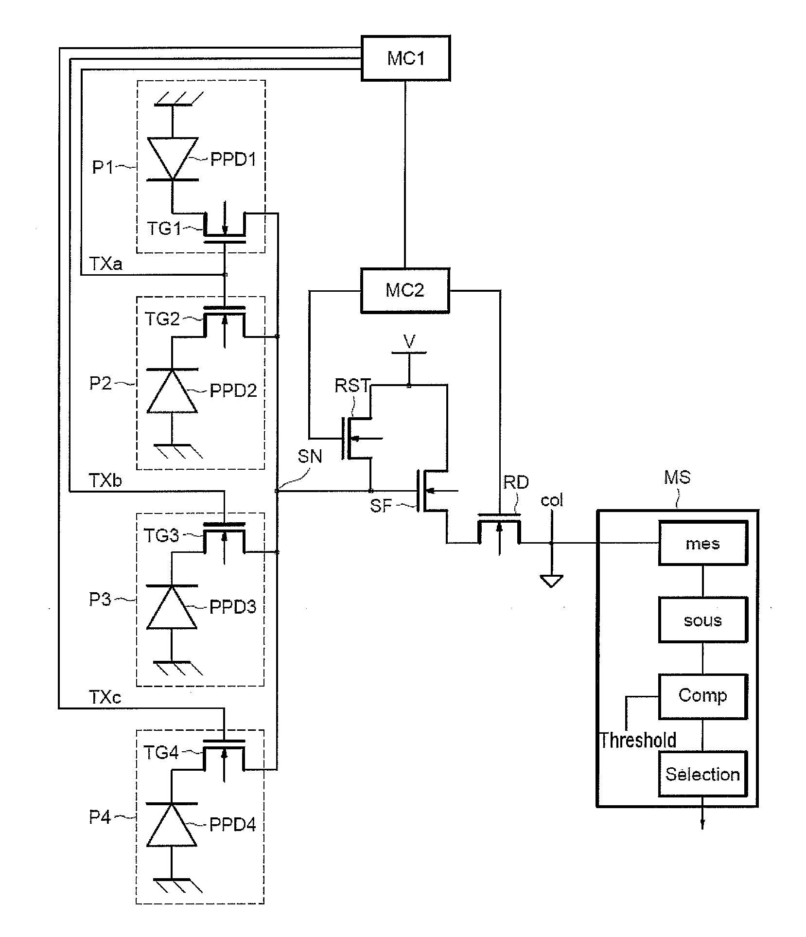
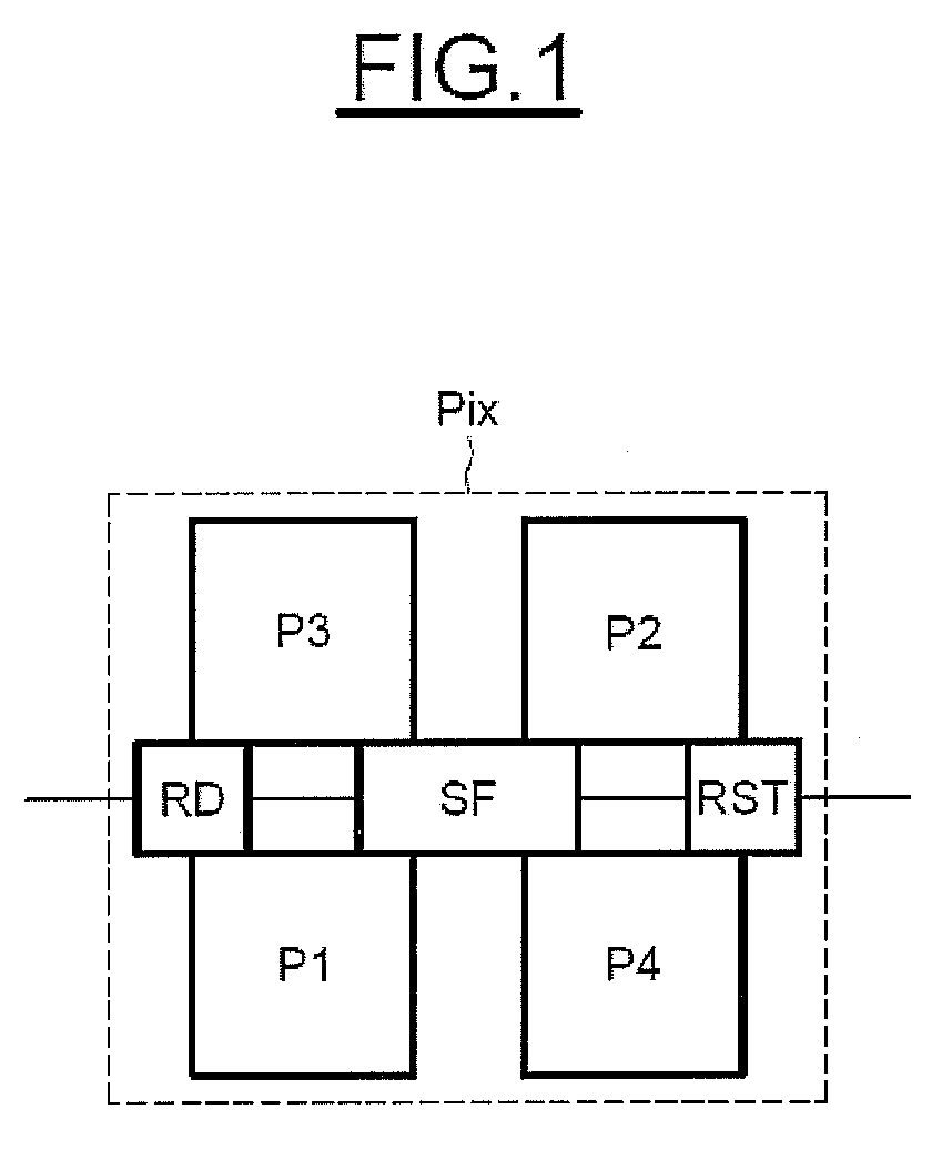
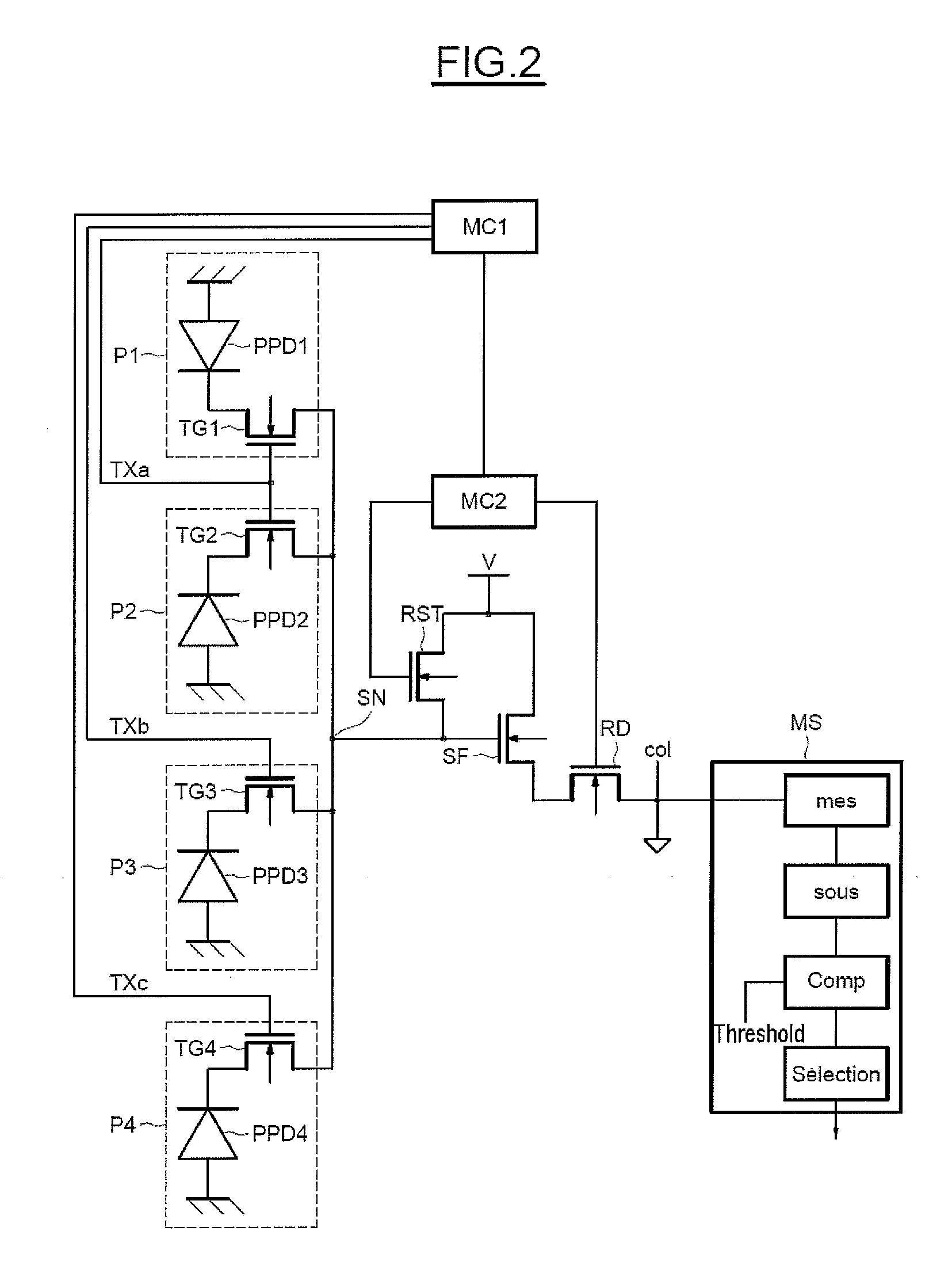
[0042]FIG. 3 illustrates an example of a method for controlling a pixel as illustrated in FIGS. 1 and 2 according to a In a first step 301, the photodiodes PPD1 and PPD2 of the first and second photosites P1 and P2 are reset. In order to reset the photodiodes PPD1 and PPD2, the second controller MC2 imposes an off-state potential, for example, 0, on the gate of the reset transistor RST as illustrated in FIG. 4 showing a timing diagram of the method. The first controller MC1 then imposes an on-state potential, for example, 1, on the gates of the charge-transfer transistors TG1 and TG2 respectively associated with the photodiodes PPD1 and PPD2 via the integration control signal TX1 for a short time so as to transfer the charges accumulated in the photodiodes P1 and P2 to the read node SN. Once the charge-transfer transistors TG1 and TG2 are again off-state, the second controller MC2 imposes an on-state potential, for example, 1, on the gate of the reset transistor RST so as to discha...

second embodiment

[0050]FIG. 5 illustrates an example of a method for controlling a pixel as illustrated in FIGS. 1 and 2 according to a The steps 501 to 507 are identical to the steps 301 to 307. Thus, in a first step 501, the photodiodes PPD1 and PPD2 of the first and second photosites P1 and P2 are reset. After step 502, photogenerated charges are accumulated in the photodiodes PPD1 and PPD2 of the first photosite and of the second photosite P1 and P2 coupled together during a first period. Then, in a step 503, the photodiode PPD3 of the third photosite P3 is reset before accumulating, in a step 504, photogenerated charges in the photodiode PPD3 of the third photosite P3 during a second period shorter than the first period. In a step 505, the photodiode PPD4 of the fourth photosite P4 is reset before accumulating, in a step 506, photogenerated charges in the photodiode of the fourth photosite P4 during a third period shorter than the second period.

[0051]In a next step 507, the read transistor RD ...


PUM


Abstract

A method for controlling a pixel may include first and second photosites, each having a photodiode and a charge-transfer transistor, a read node, and an electronic read element, all of which are common to all the photosites. The method may include an accumulation of photogenerated charges in the photodiode of the first photosite during a first period, an accumulation of photogenerated charges in the photodiode of the second photosite during a second period shorter than the first period, a selection of the signal corresponding to the quantity of charges accumulated in the photodiode of a photosite having the highest unsaturated intensity or else a saturation signal, and a digitization of the selected signal.

Description

FIELD OF THE INVENTION [0001]The invention relates to imaging devices with a matrix network of photosites and, more particularly, with multiple photosensitivity types.BACKGROUND OF THE INVENTION[0002]An imaging device, or sensor, is a photosensitive electronic component used to convert an electromagnetic ray into an analog electrical signal. This signal is then amplified and digitized by an analog-digital converter and finally processed to obtain a digital image. The imaging device makes use of the photoelectric effect. An imaging device usually comprises photosites arranged in a matrix, each photosite corresponding to a pixel of an image.[0003]A photosite comprises at least one photosensitive zone, notably a photodiode, and a zone for reading the charges accumulated in the photodiode. The photons sensed by a photodiode of a photosite are converted into electron / hole pairs. The charges of a first type, for example, the holes, created in the photosensitive zones are drained at depth ...

Claims


Application Information

Patent Timeline
Patent Type & Authority Applications(United States)
IPC IPC(8): H01L27/148
CPCH04N5/335H04N5/37457H04N5/35554H04N25/00H04N25/583H04N25/778
Inventor BARBIER, FREDERICLALANNE, FREDERIC
Owner STMICROELECTRONICS (CROLLES 2) SAS
Why Eureka
Try Eureka