Semiconductor device

Active Publication Date: 2012-12-06
SEMICON ENERGY LAB CO LTD
View PDF2 Cites 36 Cited by
  • Summary
  • Abstract
  • Description
  • Claims
  • Application Information

AI Technical Summary

Benefits of technology

[0020]The first to fourth transistors are provided in the unit cell including the analog element and the output of the unit cell is controlled by the potentials supplied to the nodes of the transistors, whereby the output of the unit cell can be switched simply and accurately. Further, when a plurality of unit cells are provided in the programmable circuit and the output of each unit cell is controlled, an analog value that can be synthesized by the programmable circuit can be variable; therefore, the circuit can

Problems solved by technology

In recent years, the reduction in power consumption of electronic devices has been an important issue, and lower power consumption of semiconductor integrated circuits used in electronic devices has also been strongly required.
However, since electrons are injected into a floating gate to write data, a hig

Method used


Image

  • Semiconductor device
  • Semiconductor device
  • Semiconductor device

Examples


embodiment 1

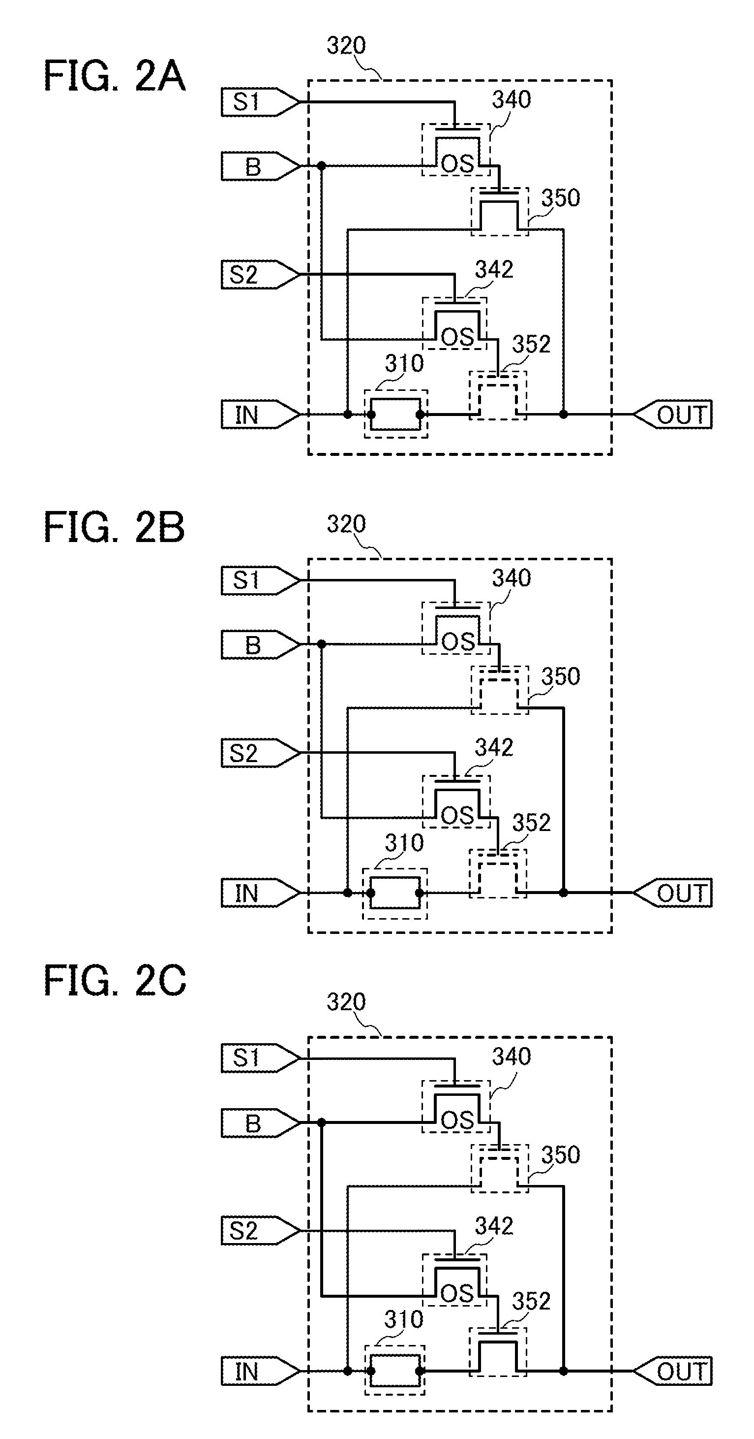
[0054]In this embodiment, a circuit configuration of a semiconductor device according to one embodiment of the disclosed invention will be described with reference to FIG. 1 and FIGS. 2A to 2C.

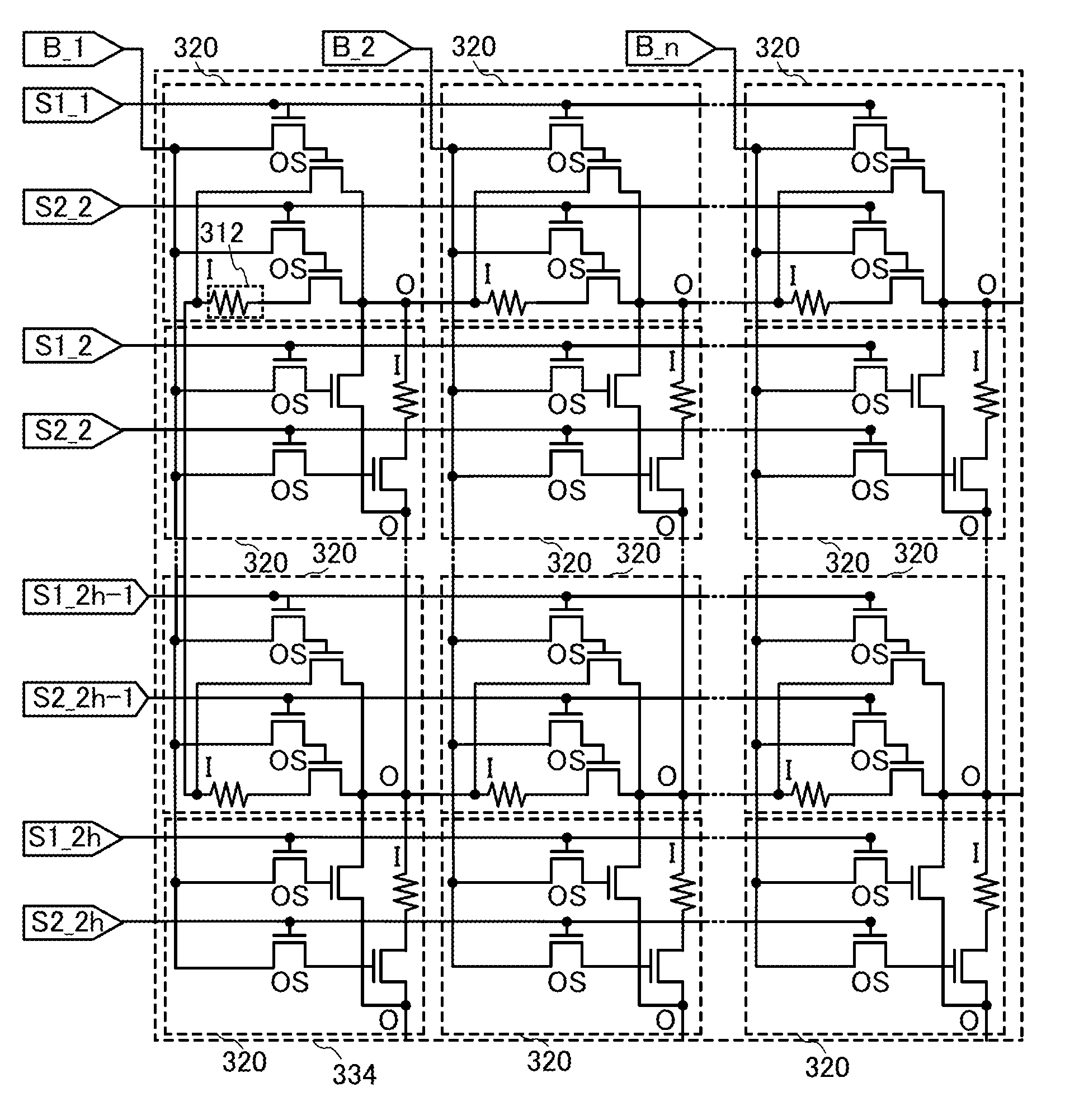
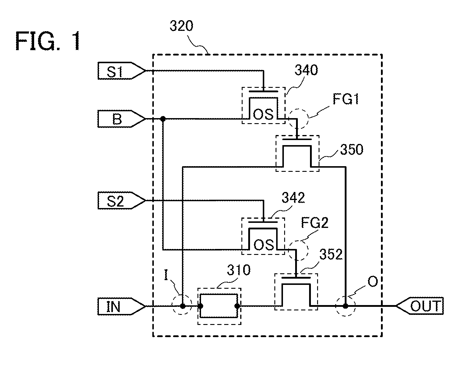
[0055]FIG. 1 illustrates a configuration of a unit cell 320 included in a programmable circuit of this embodiment.

[0056]The unit cell 320 is electrically connected to a bit line B, a unit cell selection line S1, an analog element selection line S2, an input signal line IN, and an output signal line OUT.

[0057]The unit cell 320 includes a first transistor 340, a second transistor 350, a third transistor 342, a fourth transistor 352, and an analog element 310. In the unit cell 320 in FIG. 1, the unit cell selection line S1 and a gate electrode of the first transistor 340 are electrically connected to each other and the bit line B, one of a source electrode and a drain electrode of the first transistor 340, and one of a source electrode and a drain electrode of the third transistor 342 are electri...

embodiment 2

[0099]In this embodiment, an application example of the programmable circuit 332 in Embodiment 1 will be described. Needless to say, an analog element described in this embodiment can be applied to the programmable circuit 330. Further, an analog element other than that described in this embodiment can be applied to the programmable circuit according to one embodiment of the present invention.

[0100]FIG. 5A illustrates an example where the programmable circuit 332 in FIG. 4 is applied to a ladder resistor circuit. A programmable circuit 334 illustrated in FIG. 5A includes a resistor 312 as the analog element 310 included in the unit cell 320.

[0101]In the programmable circuit 334 in FIG. 5A, the output of the unit cell can switch between a conducting state, a non-conducting state, and a conducting state through the resistor 312 by controlling the potential of the first node FG1 (where the first transistor 340 and the second transistor 350 are connected) and the potential of the second...

embodiment 3

[0107]In this embodiment, a method for manufacturing transistors included in the programmable circuit in Embodiment 1 or Embodiment 2 will be described with reference to FIGS. 6A to 6D, FIGS. 7A and 7B, FIGS. 8A to 8C, and FIGS. 9A and 9B. In this embodiment, a method for manufacturing a transistor 110 including an oxide semiconductor (hereinafter also referred to as an oxide semiconductor transistor) and an n-channel transistor 112 is specifically described as an example. Note that the oxide semiconductor transistor 110 corresponds to the first transistor 340 in FIG. 1, and the n-channel transistor 112 corresponds to the second transistor 350 in FIG. 1. In FIGS. 6A to 6D, FIGS. 7A and 7B, FIGS. 8A to 8C, and FIGS. 9A and 9B, the cross section along A-B is a cross-sectional view of a region where the oxide semiconductor transistor 110 and the n-channel transistor 112 are formed, and the cross section along C-D is a cross-sectional view of a node FG where one of a source electrode an...


PUM


Abstract

A programmable analog device and an analog device that can retain data even when supply of a power supply potential is interrupted and consumes less power. In a semiconductor device, first to fourth transistors are used as switches in a unit cell including an analog element, and the output of the unit cell switches between a conducting state, a non-conducting state, and a conducting state through the analog element by controlling the potential of a first node where the first transistor and the second transistor are connected and the potential of a second node where the third transistor and the fourth transistor are connected.

Description

BACKGROUND OF THE INVENTION[0001]1. Field of the Invention[0002]The invention disclosed in this specification relates to semiconductor devices.[0003]Note that a semiconductor device in this specification and the like refers to any device that can function by utilizing semiconductor characteristics, and semiconductor elements, electro-optical devices, storage devices, signal processing units, semiconductor circuits, and electronic devices are all semiconductor devices.[0004]2. Description of the Related Art[0005]The configurations of semiconductor integrated circuits typified by LSIs are fixed at the time of manufacture and cannot be generally changed after manufacture. In contrast, in semiconductor integrated circuits called programmable logic devices (PLDs), a logic block composed of a plurality of logic circuits is considered as a unit and logic blocks are electrically connected to each other through wirings. In a programmable logic device, the circuit configuration of each logic ...

Claims


Application Information

Patent Timeline
IPC IPC(8): H03K19/177H01L25/00
CPCH03K19/17744H01L25/00H03K19/0013H03K19/177H01L2924/0002H01L2924/00
Inventor OHMARU, TAKURO
Owner SEMICON ENERGY LAB CO LTD
Why Eureka
Try Eureka