Programmable logic device

a logic device and programmable logic technology, applied in logic circuits using specific components, pulse techniques, instruments, etc., can solve the problems of limited number of times of rewriting and and achieve the reduction of power consumption, the effect of improving processing speed and reducing the deterioration of memory elements

Active Publication Date: 2012-12-06
SEMICON ENERGY LAB CO LTD
View PDF5 Cites 13 Cited by
  • Summary
  • Abstract
  • Description
  • Claims
  • Application Information

AI Technical Summary

Benefits of technology

[0019]According to an embodiment of the present invention, deterioration of a memory element due to repeated rewriting of configuration data can be reduced. Further, a connection state of logic circuits can be kept even while power supply voltage is not supplied.
[0020]Further, according to an embodiment of the present invention, in a programmable logic device, improvement in processing speed and reduction in power consumption at the time of switching between stop and restart of supply of power supply voltage can be achieved.

Problems solved by technology

However, it is necessary to change a phase of a ferroelectric material included in a memory element at the time of writing configuration data, and the number of times of rewriting is limited.
Accordingly, deterioration of the memory element due to repeated rewriting of configuration data is a problem.

Method used


Image

  • Programmable logic device
  • Programmable logic device
  • Programmable logic device

Examples


embodiment 1

[0053]In this embodiment, a circuit structure of a programmable logic device according to an embodiment of the disclosed invention will be described with reference to FIGS. 1A and 1B, FIG. 2, FIG. 3, FIG. 4, and FIG. 5.

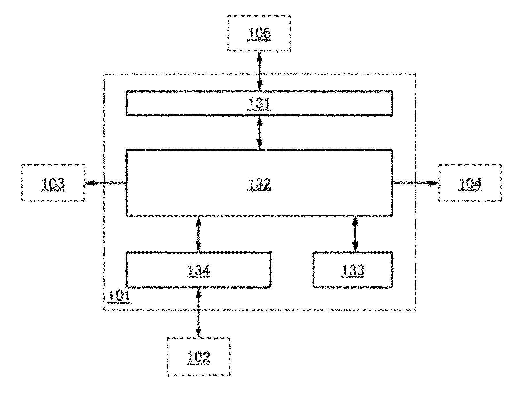
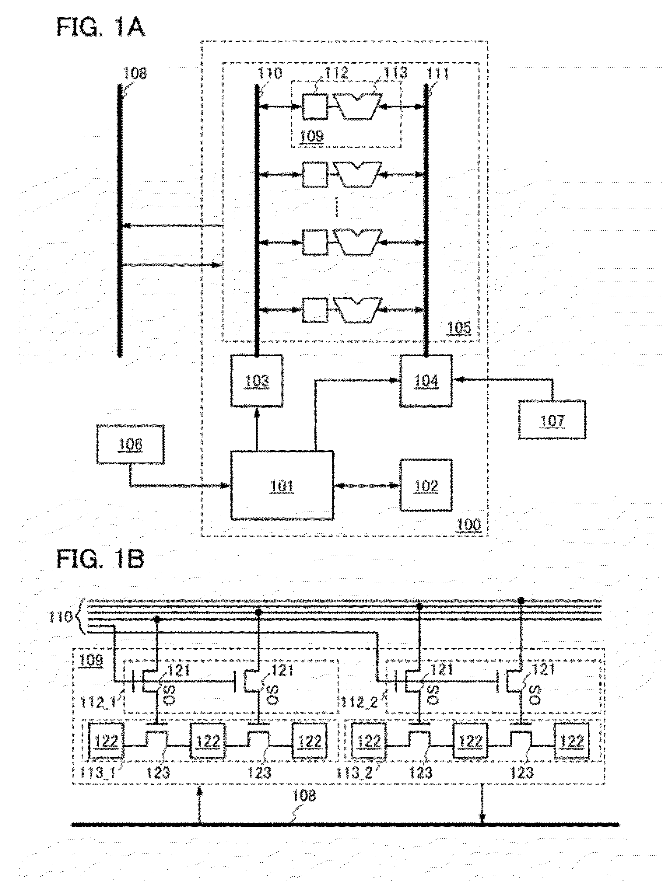
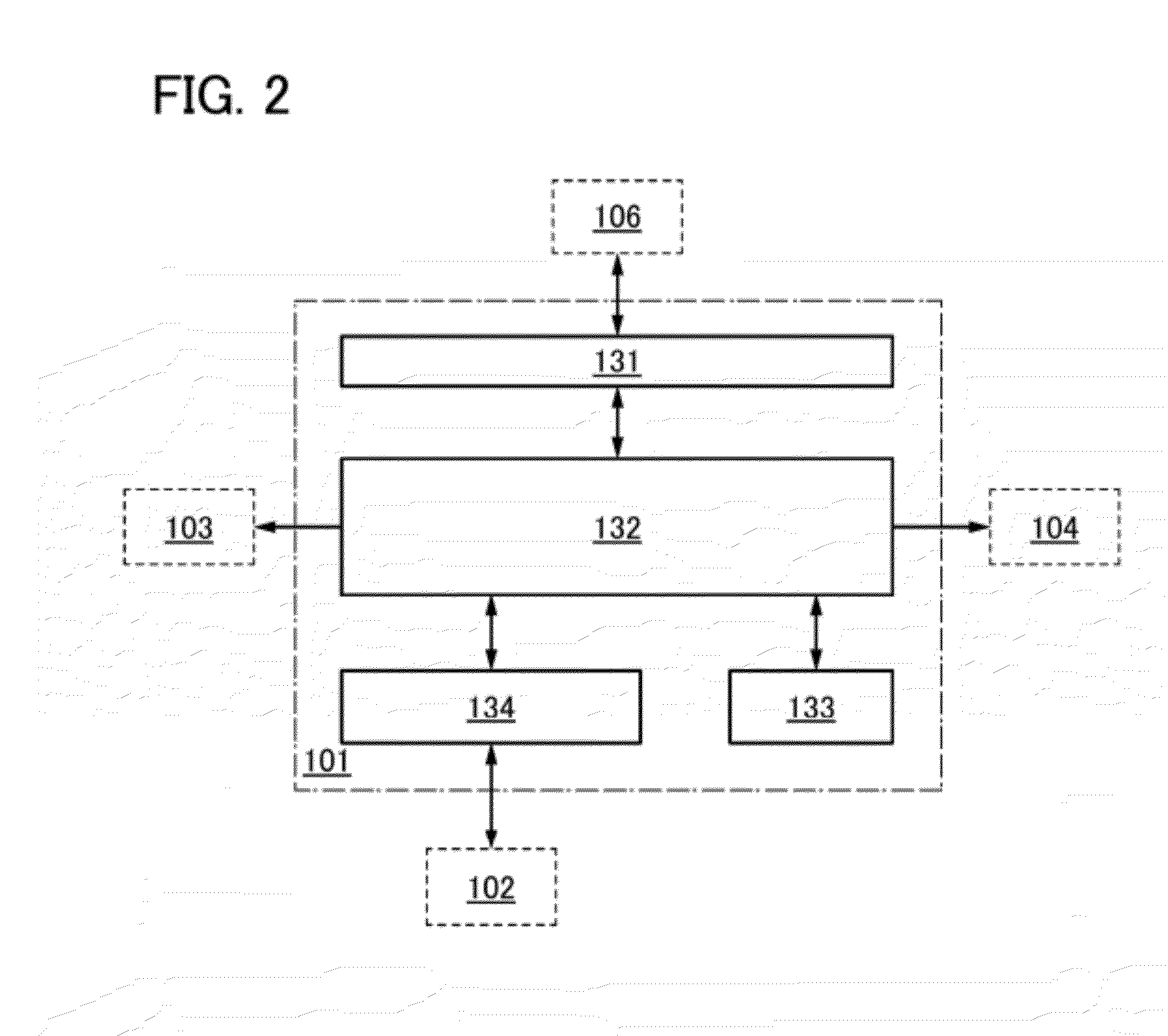
[0054]FIG. 1A illustrates a structure of a programmable logic device. A programmable logic device 100 includes an arithmetic state control circuit 101, a state memory circuit 102, a configuration changing circuit 103, a power supply control circuit 104, and an arithmetic circuit portion 105.

[0055]The arithmetic state control circuit 101 controls the configuration changing circuit 103 and the power supply control circuit 104 in accordance with an instruction signal (command signal) from a command decoder circuit 106 and data stored in the state memory circuit 102. Note that the command decoder circuit 106 analyzes a signal from the outside of the programmable logic device 100 and sends the instruction signal corresponding to the signal from the outside to the arithmeti...

embodiment 2

[0139]In this embodiment, a method for manufacturing the transistors included in the programmable logic device in Embodiment 1 will be described with reference to FIGS. 10A to 10D, FIGS. 11A and 11B, FIGS. 12A to 12C, and FIGS. 13A and 13B. As an example, a method for manufacturing the transistor 121, the transistor 171_A, and the transistor 171_B illustrated in FIG. 6C is described. Note that in FIGS. 10A to 10D, FIGS. 11A and 11B, FIGS. 12A to 12C, and FIGS. 13A and 13B, cross-sectional view taken along line A-B corresponds to a cross-sectional view of a region where the transistor 121 in which a channel formation region is formed in an oxide semiconductor, the n-channel transistor 171_A, and the p-channel transistor 171_B are formed, and a cross-sectional view taken along line C-D corresponds to a cross-sectional view of the node 172 at which the one of the source electrode and the drain electrode of the transistor 121 in which a channel formation region is formed in an oxide sem...

embodiment 3

[0274]In this embodiment, the field-effect mobility of the above-described transistor in which a channel formation region is formed in an oxide semiconductor is theoretically calculated, and the transistor characteristics are calculated from the field-effect mobility.

[0275]The actually measured field-effect mobility of an insulated gate transistor can be lower than its original mobility because of a variety of reasons; this phenomenon occurs not only in the case of using an oxide semiconductor. One of the reasons that reduce the mobility is a defect inside a semiconductor or a defect at an interface between the semiconductor and an insulating film. When a Levinson model is used, the field-effect mobility on the assumption that no defect exists inside the semiconductor can be calculated theoretically.

[0276]Assuming that the original mobility and the measured field-effect mobility of a semiconductor are μ0 and μ, respectively, and a potential barrier (such as a grain boundary) exists ...


PUM


Abstract

An object is to provide a programmable logic device configured to keep a connection state of logic circuits even while power supply voltage is stopped. The programmable logic device includes arithmetic circuits each of whose logic state can be changed; a configuration changing circuit changing the logic states of the arithmetic circuits; a power supply control circuit controlling supply of power supply voltage to the arithmetic circuits; a state memory circuit storing data on the logic states and data on states of the power supply voltage of the arithmetic circuits; and an arithmetic state control circuit controlling the configuration changing circuit and the power supply control circuit in accordance with the data stored in the state memory circuit. A transistor in which a channel formation region is formed in an oxide semiconductor layer is provided between the configuration changing circuit and each of the arithmetic circuits.

Description

BACKGROUND OF THE INVENTION[0001]1. Field of the Invention[0002]The present invention relates to a programmable logic device in which a connection state can be kept even while power is not supplied.[0003]2. Description of the Related Art[0004]Since a design of a logic circuit in a programmable logic device (PLD) can be changed by a user after the PLD is released on the market, the PLD is used in a variety of products from a prototype to a mass-produced product.[0005]A field programmable gate array (FPGA) is a typical PLD. The FPGA includes a plurality of logic circuits, and on and off of a switch which changes a connection state of the logic circuits are controlled in accordance with data (configuration data) stored in a memory portion. Thus, a logic state of the FPGA can be changed even after its manufacture.[0006]In recent years, a programmable logic device in which a connection state of logic circuits can be kept even while power supply voltage is not supplied has been actively r...

Claims


Application Information

Patent Timeline
Patent Type & Authority Applications(United States)
IPC IPC(8): G06F1/32
CPCG06F1/3243H03K19/173H03K19/17772Y02D10/00G11C15/04H01L21/82G06F3/0679
Inventor YONEDA, SEIICHIKOYAMA, JUNSHIONOIRI, YUTAKAENDO, MASAMIDEMBO, HIROKINISHIJIMA, TATSUJIKOBAYASHI, HIDETOMOOHSHIMA, KAZUAKI
Owner SEMICON ENERGY LAB CO LTD
Why Eureka
Try Eureka