Semiconductor diode

a technology of diodes and semiconductors, applied in the field of semiconductor diodes, can solve the problems of increasing the current application loss, deteriorating etc., and achieve the effect of improving the reverse withstand voltage property

Inactive Publication Date: 2012-12-13
HITACHI METALS LTD
View PDF4 Cites 6 Cited by
  • Summary
  • Abstract
  • Description
  • Claims
  • Application Information

AI Technical Summary

Benefits of technology

[0026]According to the present invention, the semiconductor diode capable of greatly improving the reverse withstand voltage property without inviting the increase of the on-resistance, can be obtained.

Problems solved by technology

However, it is conventionally considered that an effect obtained by employing the field plate structure by the aforementioned pn-junction diode is specific to the planar structure in which the electric field is concentrated to the pn-junction portion in the vicinity of the surface, and such an effect is not applied to a simple pn-junction structure in which the cathode electrode is formed on a rear surface side of a substrate, and in order to improve the reverse withstand voltage property, there is no method but reducing a carrier concentration of a p-type layer and an n-type layer, and weakening a field intensity over an entire body of the pn-junction portion.
However, a method for reducing a carrier concentration involves a problem of increasing on-resistance of the pn-junction diode, thus increasing the current application loss.
Further, a lattice defect in the crystal is also considered to be one of the causes of deteriorating the reverse withstand voltage property.
Also, it is considered that inherent defect level and impurity level are generated in the lattice defect, and a current is leaked in a reverse direction through these levels, and there is no method but improving the crystal itself for improving the reverse withstand voltage property.

Method used


Image

  • Semiconductor diode
  • Semiconductor diode
  • Semiconductor diode

Examples


examples

[0044]Examples of the present invention will be described next.

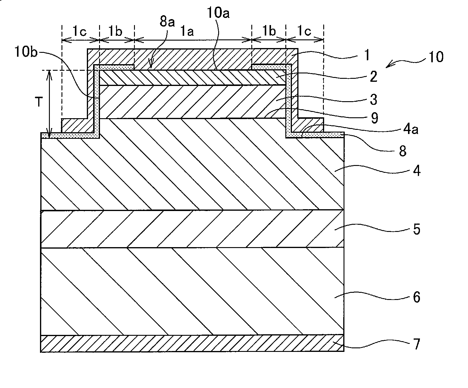
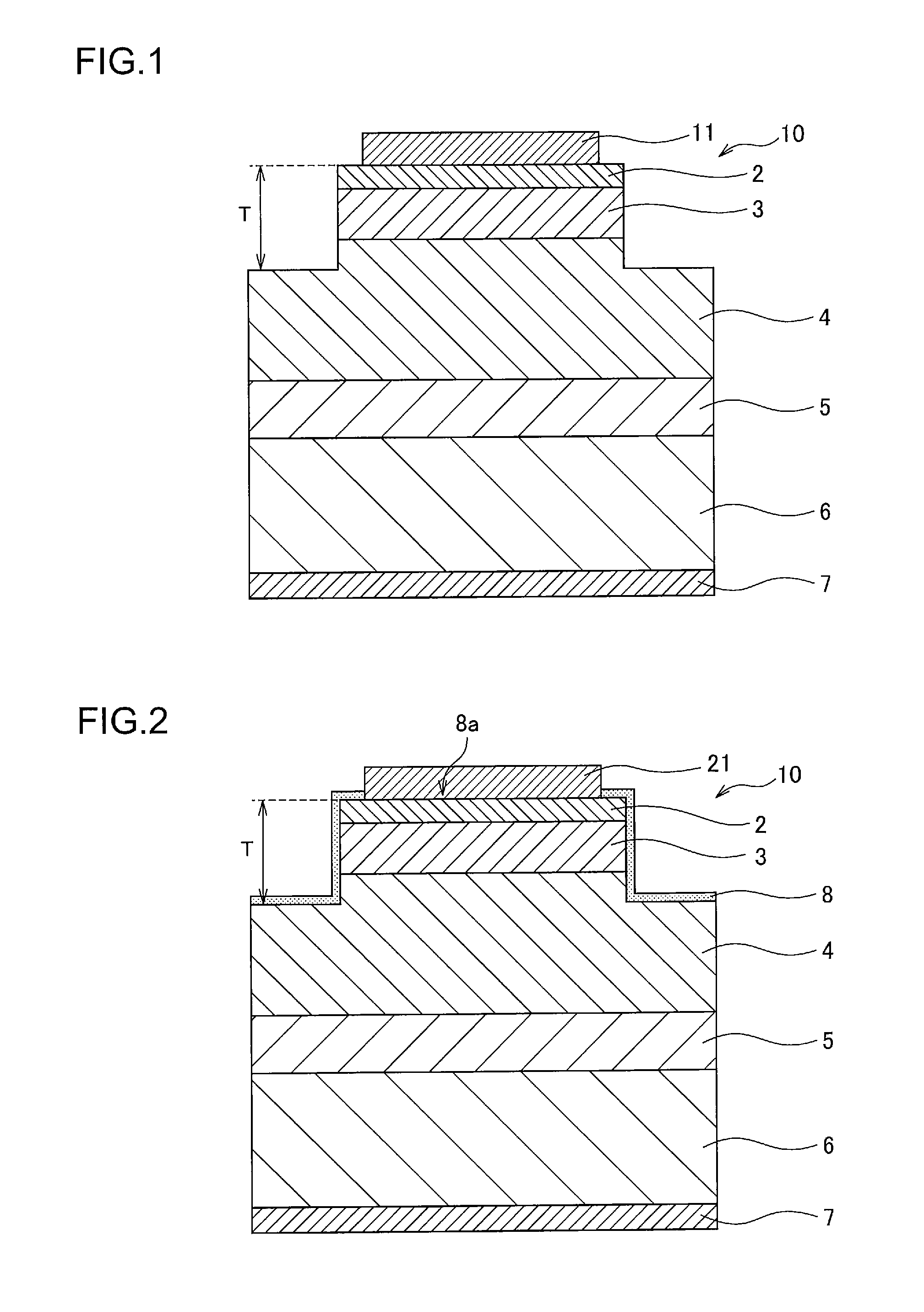
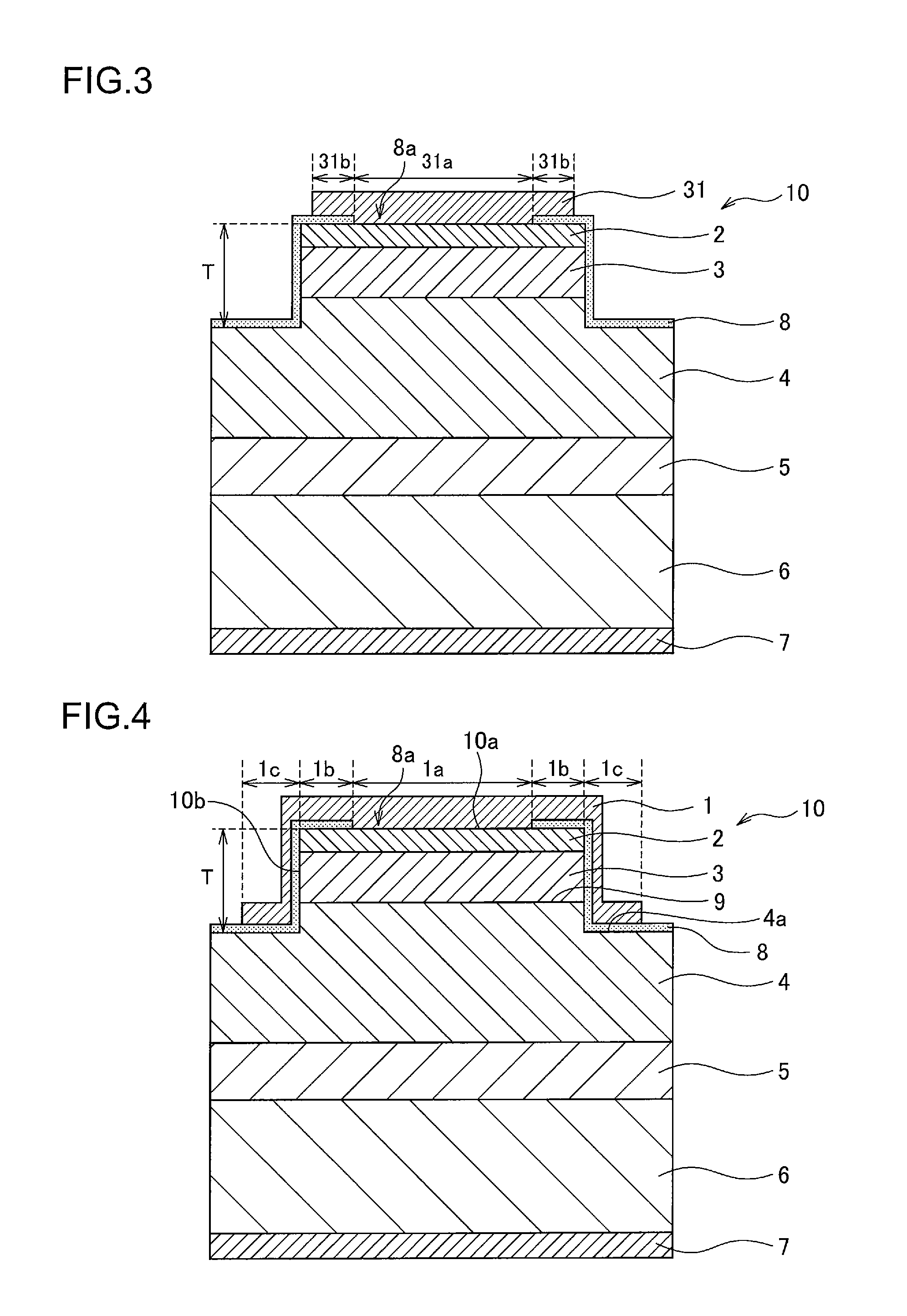
[0045]The semiconductor diode according to an example of the present invention has a structure similar to the structure of the semiconductor diode according to the aforementioned embodiment shown in FIG. 4. Therefore, the semiconductor diode according to this example will be described using FIG. 4. Further, semiconductor diodes of comparative examples 1, 2, 3 to be compared and evaluated with this example, are shown in FIG. 1, FIG. 2, and FIG. 3 respectively.

example

[0046]A method for manufacturing the semiconductor diode of the example of the present invention will be described.

[0047]First, as a substrate, a low dislocation-density (about 106 / cm2) n-type GaN substrate (carrier concentration: 1×10¹⁸ / cm3, thickness: 400 μm) 6 was prepared using a Void-Assisted Separation, (VAS) method. Then, Si-doped n-type GaN layers 5, 4 and Mg-doped p-type GaN layers 3, 2 were laminated on the n-type GaN substrate 6 using a Metal Organic Chemical Vapor Deposition Epitaxy (MOVPE) method, to thereby form a semiconductor lamination portion. The structure of each layer of the semiconductor lamination portion is as follows. Namely, the n-type GaN layer 5 has a Si concentration of 2×10¹⁸ / cm3, a thickness of 2 μm, and the n-type GaN layer 4 has a Si concentration of 2×10¹⁶ / cm3 and a thickness of 10 μm, and the p-type GaN layer has a Mg concentration of 2×10¹⁹ / cm3 and a thickness of 500 nm, and the p-type GaN layer 2 has a Mg concentration of 2×10²⁰ / cm3 and a thickne...


PUM


Abstract

To provide a semiconductor diode with a part of a semiconductor lamination portion having a mesa structure portion, which is the part where a pn-junction is formed by lamination of an n-type semiconductor layer and a p-type semiconductor layer on a substrate, comprising: a protective insulating film formed by coating a main surface of the mesa structure portion, a side face of the mesa structure portion in which an interface of the pn-junction is exposed, and an etched and exposed surface of the n-type semiconductor layer; and an anode electrode formed in ohmic-contact with the p-type semiconductor layer exposed from an opening formed on a part of the main surface of the mesa structure portion of the protective insulating film, extending from the main surface, through the side face of the mesa structure portion, to the surface of the n-type semiconductor layer.

Description

[0001]The present application is based on Japanese Patent Application No. 2011-128535 filed on Jun. 8, 2011, the entire contents of which are hereby incorporated by reference.TECHNICAL FIELD[0002]The present invention relates to a semiconductor diode having a pn-junction, and particularly relates to the semiconductor diode having a new anode electrode shape.DESCRIPTION OF RELATED ART[0003]A pn-junction diode using a nitride semiconductor is paid attention to as a large capacity rectifying device of the next generation, due to its high breakdown voltage and because low-current application loss can be expected.[0004]Conventionally, in an anode electrode of a Schottky Barreir Diode (SBD), a field plate structure is employed for relaxing an electric field concentration to an electrode end (for example, see patent documents 1, 2, 4), wherein a technique used in silicon SBD is applied. The field plate structure is a structure in which a protective insulating film formed on a semiconductor...

Claims


Application Information

Patent Timeline
Patent Type & Authority Applications(United States)
IPC IPC(8): H01L29/20
CPCH01L29/2003H01L29/8613H01L29/407
Inventor TSUCHIYA, TADAYOSHIKANEDA, NAOKIMISHIMA, TOMOYOSHIKAWANO, TOSHIHIRONAKAMURA, TORUNOMOTO, KAZUKI
Owner HITACHI METALS LTD
Why Eureka
Try Eureka