LED leadframe or LED substrate, semiconductor device, and method for manufacturing LED leadframe or LED substrate

a technology of led leadframe or led substrate and led substrate, which is applied in the direction of semiconductor devices, semiconductor device details, electrical devices, etc., can solve the problems of affecting the performance of the entire visible region, affecting the overall visible region, etc., to achieve efficient reflection, reduce cost, and high reflection characteristics

Active Publication Date: 2012-12-13
DAI NIPPON PRINTING CO LTD
View PDF5 Cites 96 Cited by
  • Summary
  • Abstract
  • Description
  • Claims
  • Application Information

AI Technical Summary

Benefits of technology

[0151]Then, the function and the effect of this embodiment are to be described. In the semiconductor device 20 of this embodiment, the reflection metal layer 12 serving as a reflection layer is disposed over the mounting surface 11a of the main body portion 11 as described above. The reflection metal layer 12 comprises the alloy of platinum and silver or the alloy of gold and silver. This can provide the following function and effect.
[0152]That is, after lapse of a predetermined time from the manufacture of the semiconductor device 20, a corrosive gas such as oxygen or a hydrogen sulfide gas in the air penetrates into the semiconductor device 20, for example, at a portion between the outer resin portion 23 and the encapsulating resin portion 24. According to this embodiment, the reflection metal layer 12 that serves as the reflection layer is disposed over the mounting surface 11a of the main body portion 11 and the reflection metal layer 12 comprises the alloy of platinum and silver or the alloy of gold and silver. Thus, even when the corrosive gas penetrates into the semiconductor device 20, the reflection layer (reflection metal layer 12) is less discolored or corroded and the reflectance thereof is not lowered. On the other hand, when the reflection layer is comprised only of the silver plating layer as a comparative embodiment, the reflection layer may possibly undergo discoloration or corrosion when the corrosive gas penetrates into the semiconductor device 20.
[0153]Further, according to this embodiment, since the reflection layer comprises the reflection metal layer 12 and has high reflection characteristics, light from the LED element 21 can be reflected efficiently.
[0154]Further, according to this embodiment, the reflection metal layer 12 comprises an extremely thin film (0.005 to 0.2 μm) as described above. Accordingly, the reflection metal layer 12 is fractured partially by the energy applied during die attachment or wire bonding. Accordingly, a pull strength substantially identical with that when die attaching or wire bonding is directly performed on the silver plating can be obtained.
[0155]Further, according to this embodiment, since the thickness of the reflection metal layer 12 is extremely thin, the cost less increases even when relatively expensive platinum or gold is used. Further, since the reflection metal layer 12 comprises the alloy of platinum and silver or the alloy of gold and silver, the manufacturing cost can be suppressed compared with the use of only platinum or gold for the material as the reflection metal layer 12.
[0156]Each of modified embodiments of the semiconductor device according to this embodiment is to be described with reference to FIG. 6 to FIG. 11. In FIG. 6 to FIG. 11, portions identical with those of the embodiment shown in FIG. 3 carry the same reference numerals and detailed description therefor is to be omitted.

Problems solved by technology

However, since the gas barrier property tends to be poor if the silicone resin is used, a corrosive gas such as oxygen or hydrogen sulfide gas in atmospheric air penetrates as far as the Ag layer inside the semiconductor device.
Since Ag is easily reacted with the hydrogen sulfide gas or the like to form a product such as silver sulfide, this results in a problem that an Ag layer is discolored in the appearance and the reflectance of the Ag layer is remarkably deteriorated for the entire visible region.

Method used


Image

  • LED leadframe or LED substrate, semiconductor device, and method for manufacturing LED leadframe or LED substrate
  • LED leadframe or LED substrate, semiconductor device, and method for manufacturing LED leadframe or LED substrate
  • LED leadframe or LED substrate, semiconductor device, and method for manufacturing LED leadframe or LED substrate

Examples


first embodiment

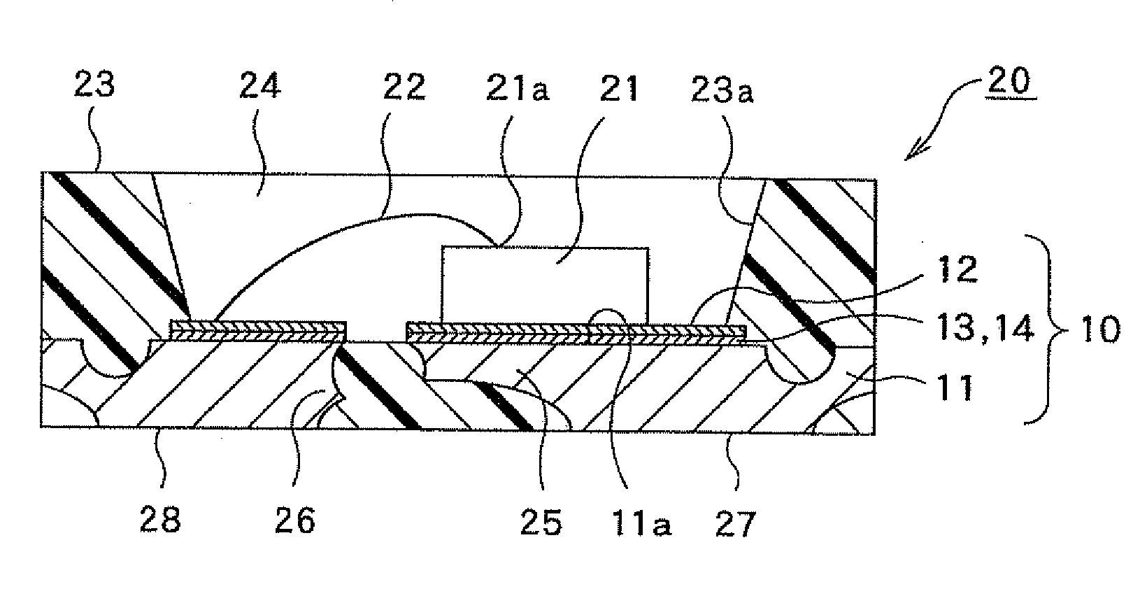
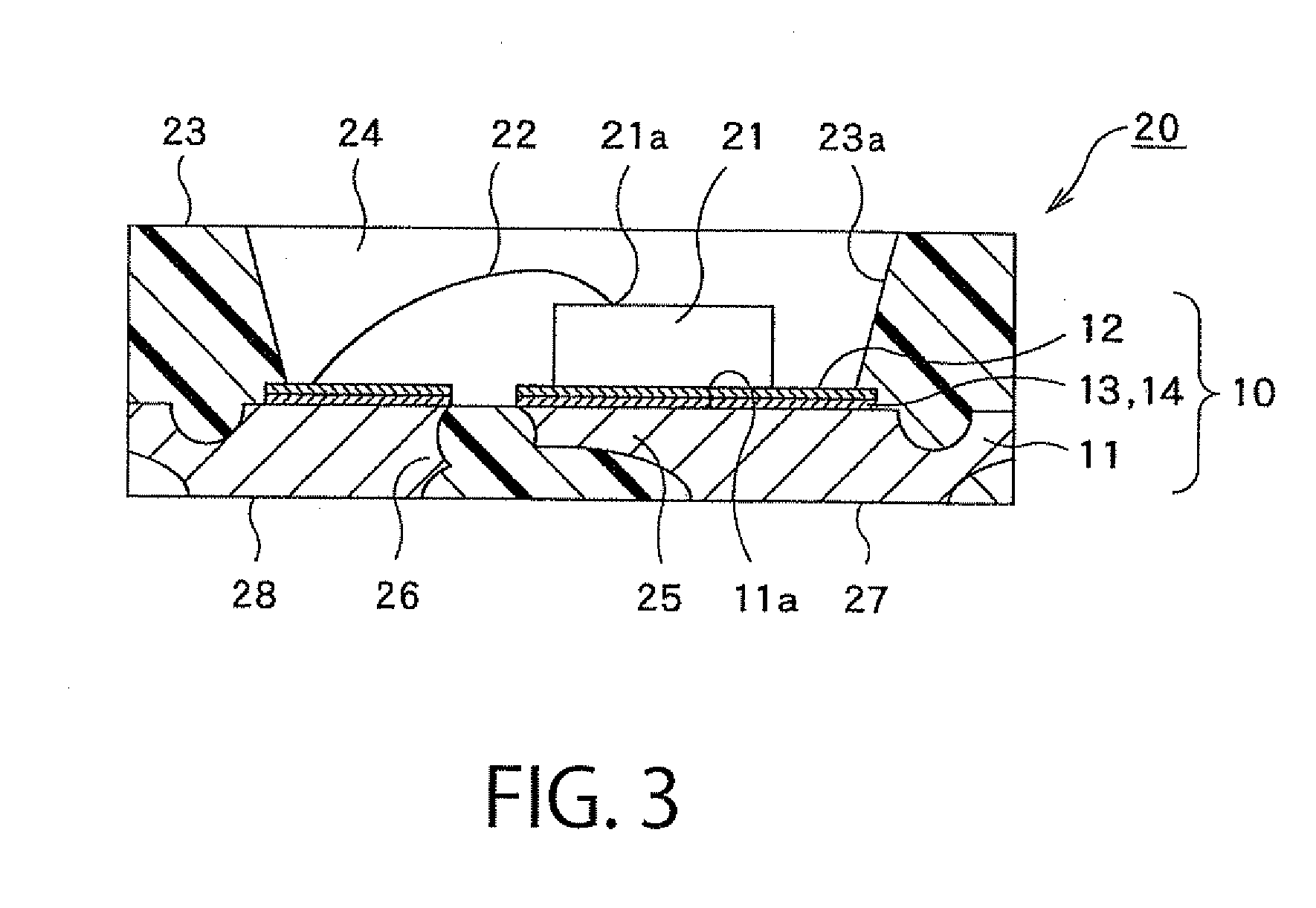
[0105]A first embodiment of the present invention is to be described with reference to FIG. 1 to FIG. 13.

Configuration of LED Leadframe or LED Substrate

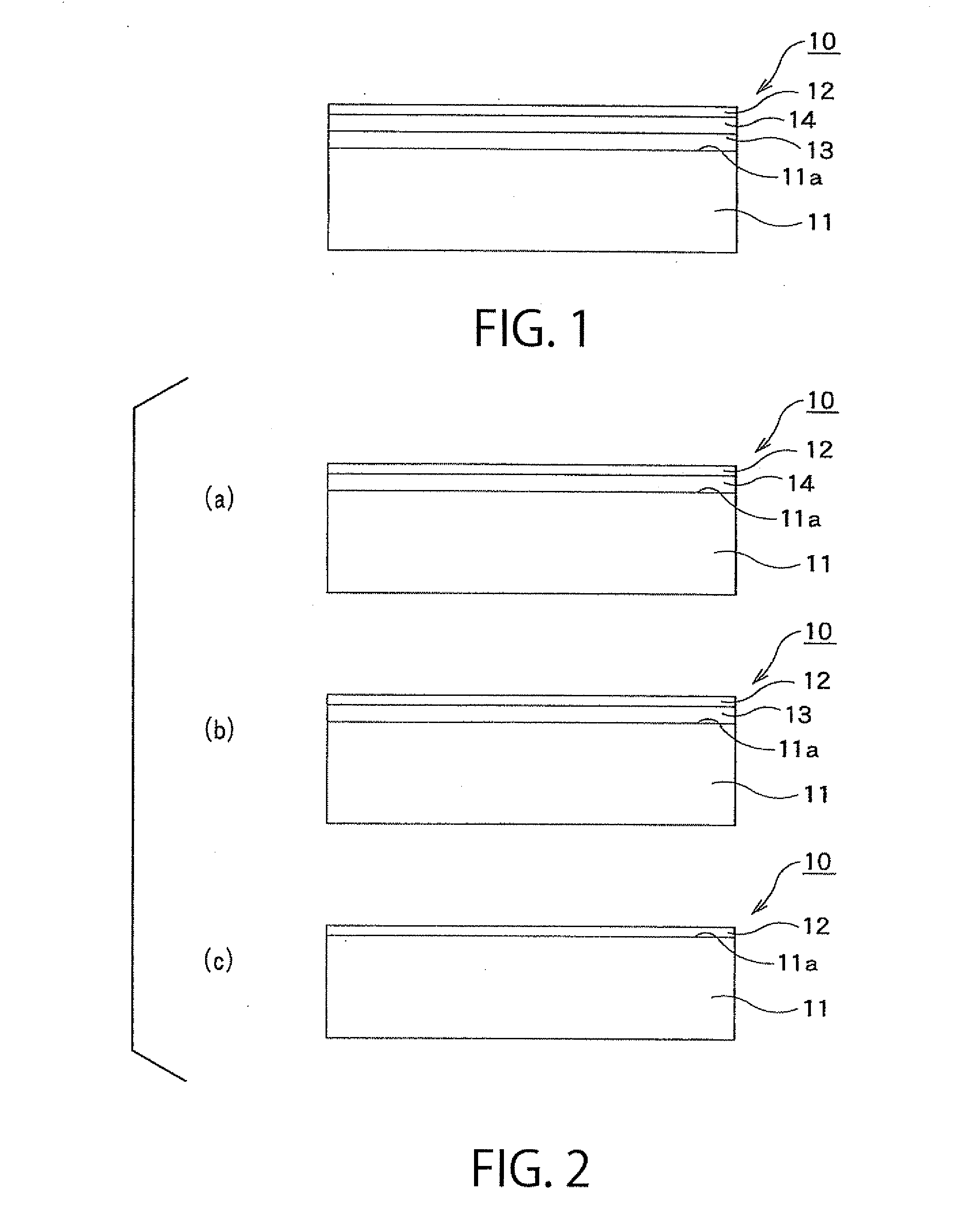
[0106]First, the outline of an LED leadframe or LED substrate is to be described with reference to FIG. 1 and FIG. 2. In FIG. 1 and FIG. 2, for the explanation of the layer configuration of the LED leadframe or LED substrate, a cross section of the LED leadframe or LED substrate is shown as a rectangular shape for the sake of convenience.

[0107]As shown in FIG. 1, an LED leadframe or LED substrate 10 according to this embodiment (hereinafter referred to also as a leadframe 10 or substrate 10) is used for mounting an LED element 21 (to be described later). The LED leadframe or LED substrate 10 includes a main body portion 11 having a mounting surface 11a for mounting the LED element 21, and a reflection plating layer 12 disposed over the mounting surface 11a of the main body portion 11.

[0108]The main body portion 11 comprises a metal p...

example 1-a

[0191]A copper plating layer 13 (0.05 μm thickness) was formed on a main body portion 11 comprising a copper plate, and a silver plating layer 14 (3 μm thickness) was applied on the copper plating layer 13. Then, a reflection metal layer 12 comprising an alloy of gold (Au) and silver (Ag) (0.1 μm thickness) was formed by plating on the silver plating layer 14, thereby manufacturing a substrate 10 (Example 1-A). In this case, the reflection metal layer 12 has a composition comprising 50% by weight of gold and the balance being silver and an inevitable impurity.

example 1-b

[0192]A substrate 10 (Example 1-B) was manufactured in the same manner as in Example 1-A except that the reflection metal layer 12 had a composition containing 30% by weight of gold and the balance being silver and an inevitable impurity.


PUM

PropertyMeasurementUnit
thicknessaaaaaaaaaa
thicknessaaaaaaaaaa
thicknessaaaaaaaaaa

Abstract

An LED leadframe or LED substrate includes a main body portion having a mounting surface for mounting an LED element thereover. A reflection metal layer serving as a reflection layer for reflecting light from the LED element is disposed over the mounting surface of the main body portion. The reflection metal layer comprises an alloy of platinum and silver or an alloy of gold and silver. The reflection metal layer efficiently reflects light emitted from the LED element and suppresses corrosion due to the presence of a gas, thereby capable of maintaining reflection characteristics of light from the LED element.

Description

TECHNICAL FIELD[0001]The present invention relates to an LED leadframe or LED substrate for mounting an LED element, and a method for manufacturing the same. The invention also relates to a semiconductor device having the LED leadframe or LED substrate, and a method for manufacturing the same.BACKGROUND ART[0002]Conventionally, illumination apparatuses using LED (light emitting diode) elements as a light source are utilized for various home appliances, office automation equipment, vehicle display lamps, general illumination, vehicle-mounted illumination, and displays. Some illumination apparatuses include a semiconductor device having an LED substrate and an LED element.[0003]Examples of the LED element include those that emit light in a visible region typically represented by red, green, and blue and an ultraviolet region. Since a wavelength distribution of the light emitted from these light emitting elements is basically narrow, it can be said that the light can be seen as a singl...

Claims


Application Information

Patent Timeline
Patent Type & Authority Applications(United States)
IPC IPC(8): H01L33/60H01L33/48
CPCH01L21/6835H01L23/49582H01L23/49861H01L24/16H01L24/29H01L24/45H01L24/48H01L24/97H01L33/486H01L33/60H01L33/62H01L2224/16225H01L2224/16245H01L2224/32245H01L2224/45144H01L2224/48091H01L2224/48247H01L2224/48465H01L2224/48599H01L2224/73265H01L2224/85439H01L2224/85444H01L2224/85469H01L2224/92247H01L2224/97H01L2924/01013H01L2924/01014H01L2924/01022H01L2924/01028H01L2924/01029H01L2924/01047H01L2924/01049H01L2924/0105H01L2924/01078H01L2924/01079H01L2924/01082H01L2924/014H01L2924/078H01L2924/10329H01L2924/1815H01L2924/01005H01L2924/01006H01L2924/01019H01L2924/01033H01L2924/0104H01L2924/01045H01L2924/01072H01L2924/01074H01L2924/12041H01L23/3121H01L24/32H01L24/81H01L24/83H01L24/85H01L2224/13144H01L2224/2919H01L2224/29101H01L2224/131H01L2224/48245H01L2924/01327H01L2224/83H01L2924/00014H01L2224/85H01L2224/81H01L2924/00H01L2924/3512H01L33/46H01L33/48H01L33/52H01L33/56H01L2933/0025H01L2933/005H01L2933/0066H01L2224/48639H01L2224/48644H01L2224/48669H01L2924/15747H01L2924/15787H01L2924/15788H01L2924/181H01L2924/00012H01L2224/48227H01L33/20H01L33/50H01L2924/1715H01L2924/3025H01L21/4828H01L21/56H01L23/49503H01L23/49541H01L2933/0058
Inventor ODA, KAZUNORISAKAMOTO, AKIRAMURATA, YOSHINORIKAWAI, KENZABUROSUZUKI, KOICHIOISHI, MEGUMI
Owner DAI NIPPON PRINTING CO LTD
Why Eureka
Try Eureka