
Semiconductor memory device

Inactive Publication Date: 2012-12-13
SHARP KK
View PDF4 Cites 7 Cited by
  • Summary
  • Abstract
  • Description
  • Claims
  • Application Information

AI Technical Summary

Benefits of technology

[0018]In view of the above-mentioned conventional problems, the present invention aims to provide a semiconductor memory device that can efficiently correct data, when a data error, which is possibly generated because the data is used after retained for a long period, is detected and corrected.
[0019]The present invention utilizes a characteristic of a variable resistive element having a metal oxide described below, thereby simplifying a writing process for correcting a data error of a memory cell.

Problems solved by technology

Therefore, the flash memory cannot be operated with high speed.
However, there arises a problem that writing by random access cannot be performed, since the erasing action is performed on a block basis.
On the other hand, there are problems to be solved, caused by the property unique to the resistance random access memory.
Accordingly, when a power supply is turned off for a long time under high-temperature environment, it is difficult to completely prevent the increased possibility of an error caused on a bit with weak data retention.
However, when the data in the memory cell is corrected, the writing action of the variable resistive element is necessary, and its process is complicated.

Method used


Image

  • Semiconductor memory device
  • Semiconductor memory device
  • Semiconductor memory device

Examples


first embodiment

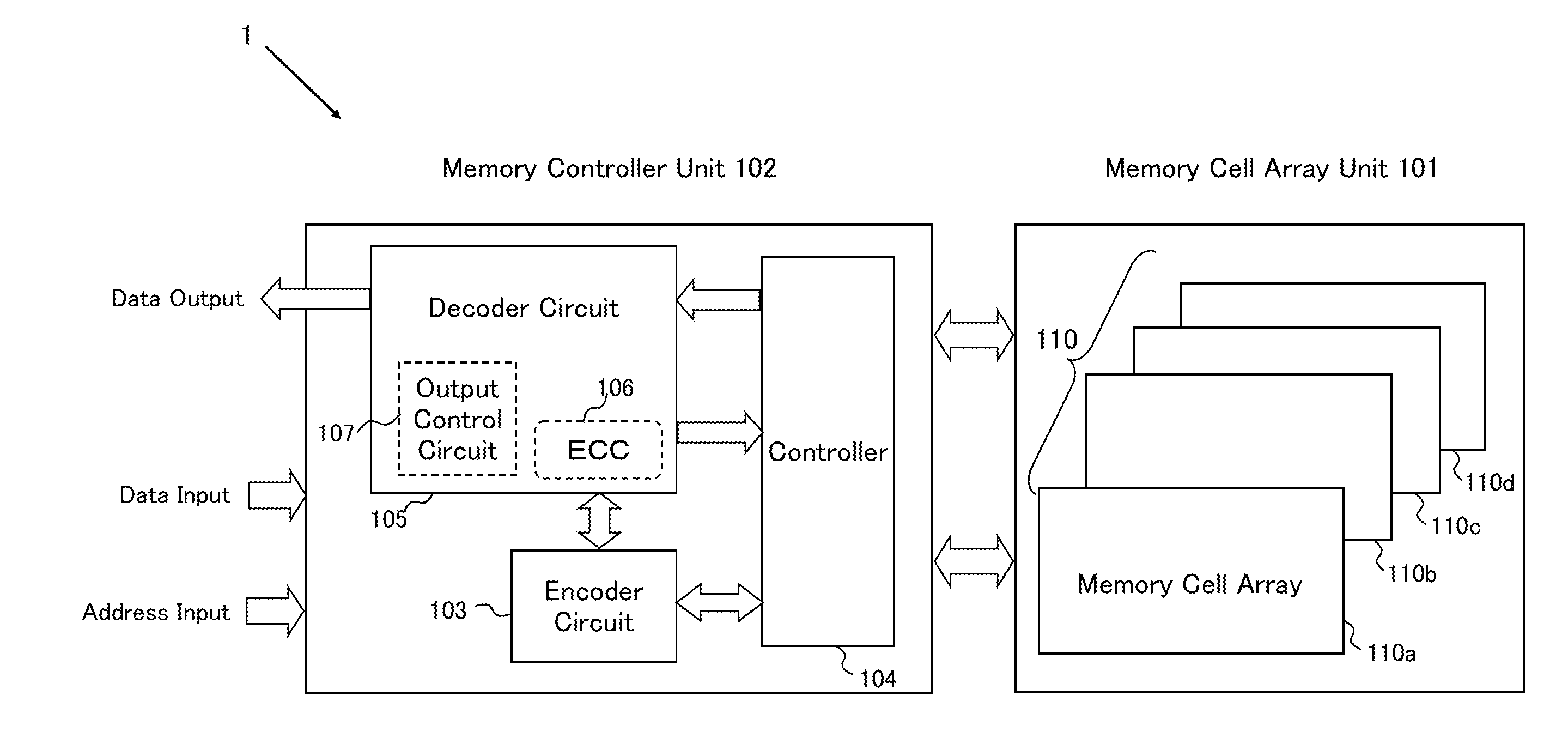
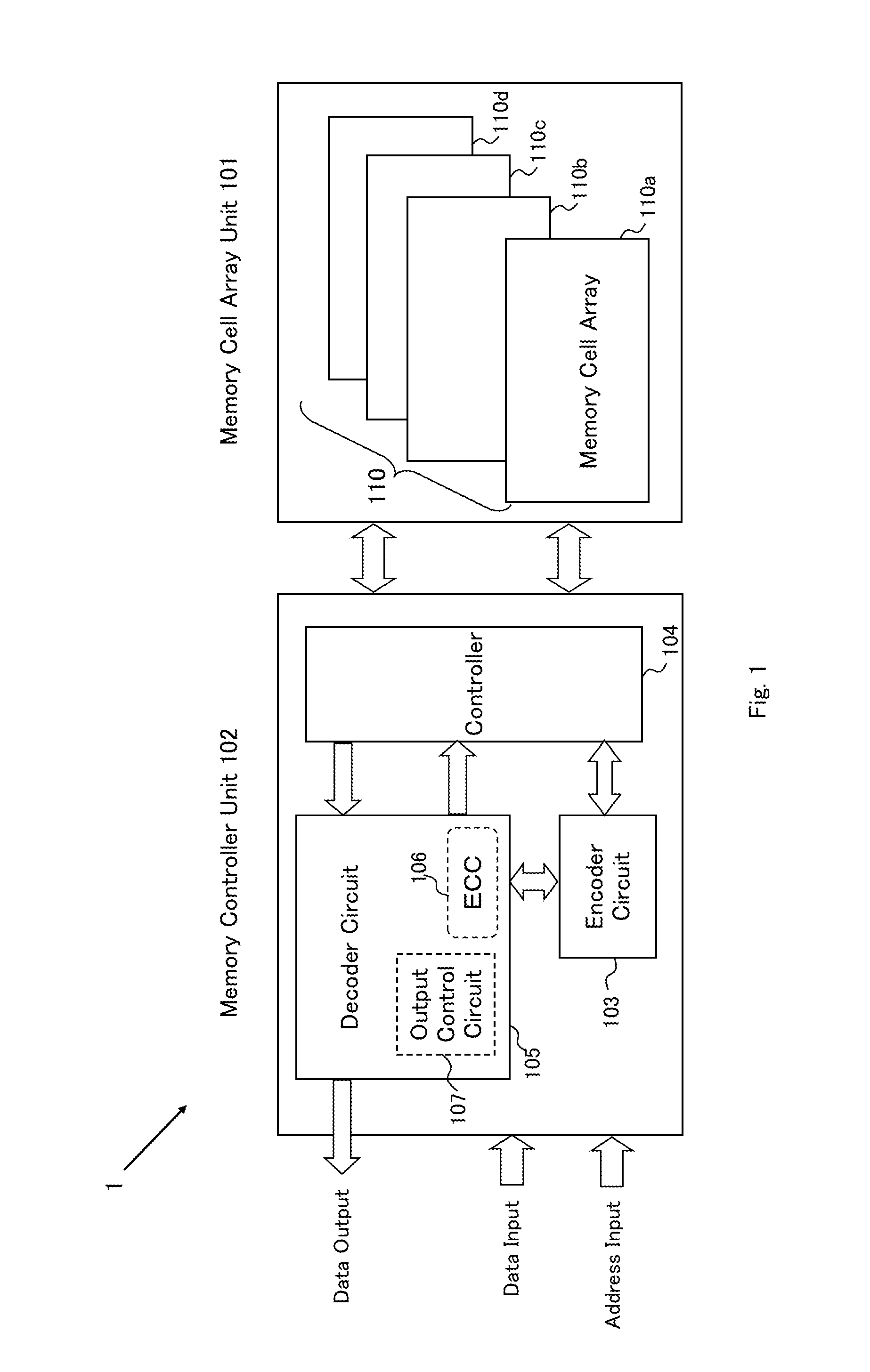
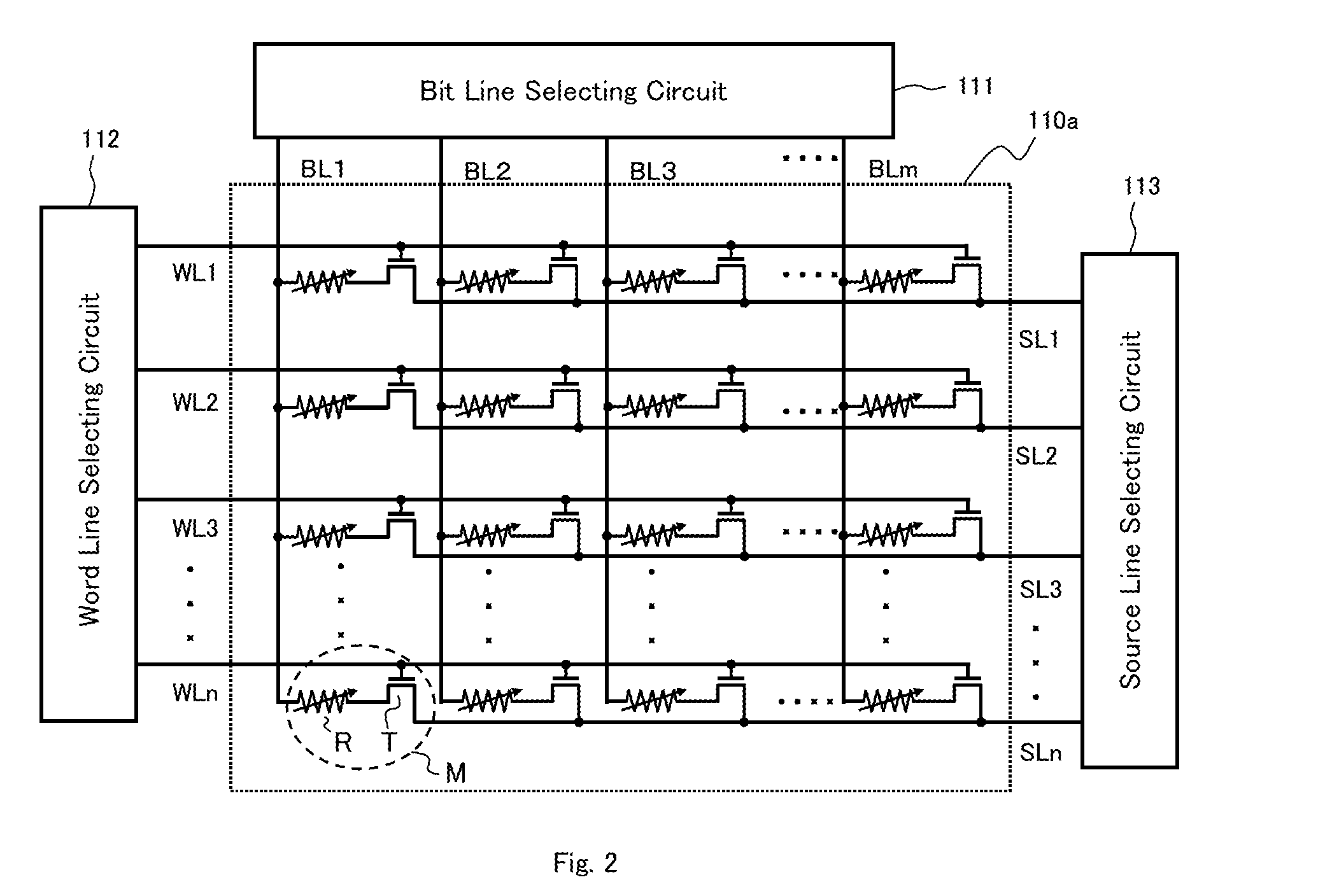
[0069]FIG. 1 shows a schematic circuit structure of a semiconductor memory device (hereinafter appropriately referred to as a “present device 1”) according to one embodiment of the present invention. The present device 1 basically includes a memory cell array unit 101, and a memory controller unit 102. The memory controller unit 102 includes an encoder circuit 103 that performs error-correction coding for adding an error-correction check bit to a plurality of information bits, which are input data, and generates coded data having a bit length longer than that of the information bits; a controller 104 that controls a writing action and a reading action of the coded data to a memory cell in the memory cell array in the memory cell array unit 101 specified by an input address; and a decoder circuit 105 that decodes the coded data (information bits+check bit) read through the controller 104, detects whether the decoded data has an error or not, and corrects the error. The decoder circui...

second embodiment

[0100]The method of detecting the error in the coded data and the method of the correction and writing by the present device 1 will be described with reference to another flowchart in FIG. 8. In the flowchart in FIG. 8, a check bit that is generated by coding the read information bits and the read check bit are compared after the reading action and before the decoding action in order to detect an error. When both check bits are consistent with each other, it is determined that there is no error, so that the error correction is not executed. Only when both check bits are not consistent with each other, the decoding action is executed to specify an address having the data error based upon the error-correction coding.

[0101]Firstly, in FIG. 8, when the address of the memory cell, which is the target of the reading action, is inputted to the memory controller unit 102 (step #300), the controller 104 in the memory controller unit 102 specifies the plurality of memory cells corresponding t...

third embodiment

[0107]As described above, when the data error is detected in the error detection action by the ECC, the present device 1 executes the first writing action to the memory cell in the memory cell array on the address where the error is detected based upon the error-correction coding. On the other hand, when the device is operated under high temperature for a long time, the possibility that an error is detected on a bit with a weak data retention increases.

[0108]FIG. 9 shows a data retention characteristic at high temperature after the resistance state is changed to the low resistance state by the first writing action in the form of a change in a cumulative probability of an error bit that cannot retain data due to an increase in the resistance value. This experiment was carried out to the variable resistive elements R corresponding to 256 bits, each of which has titanium nitride (TiN) as the first electrode, tantalum (Ta) as the second electrode, and a variable resistor that is made of...


PUM


Abstract

In a semiconductor memory device using a variable resistive element made of a metal oxide for storing information, a voltage amplitude of a writing voltage pulse for changing the variable resistive element to a high resistance state is set within a voltage range in which the resistance value of the high resistance state after the change increases with time. The voltage amplitude is set within the voltage range in which the resistance value of the high resistance state after the change increases toward a predetermined peak with increase in voltage amplitude. When a data error is detected by the ECC circuit, it is estimated that the data that should be in the low resistance state changes to the high resistance state, and the variable resistive elements of all memory cells from which the error is detected are written to the low resistance state to correct the error bit.

Description

CROSS REFERENCE TO RELATED APPLICATION[0001]This Nonprovisional application claims priority under 35 U.S.C. §119(a) on Patent Application No. 2011-128954 filed in Japan on Jun. 9, 2011 the entire contents of which are hereby incorporated by reference.BACKGROUND OF THE INVENTION[0002]1. Field of the Invention[0003]The present invention relates to a semiconductor memory device including a memory cell array that includes a plurality of memory cells in a row direction and a column direction, respectively, wherein each of the memory cells includes a variable resistive element storing information based upon an electric operating characteristic in which an electric resistance changes due to application of an electric stress.[0004]2. Description of the Related Art[0005]A non-volatile memory represented by a flash memory has widely been used for a computer, communication, measuring device, automatic control device, and device for daily use in a personal life, as a high-capacity and compact i...

Claims


Application Information

Patent Timeline
IPC IPC(8): G11C11/00
CPCG06F11/1048G11C13/004G11C2029/0411G11C13/0061
Inventor ONISHI, JUNYAAWAYA, NOBUYOSHINAKURA, MITSURUISHIHARA, KAZUYA
Owner SHARP KK
Learn More