Power Converter

a power converter and converter technology, applied in the direction of electronic switching, pulse technique, solid-state devices, etc., to achieve the effect of reducing loss, improving noise resistance, and reducing leakage curren

Active Publication Date: 2012-12-20
HITACHI ASTEMO LTD
View PDF4 Cites 16 Cited by
  • Summary
  • Abstract
  • Description
  • Claims
  • Application Information

AI Technical Summary

Benefits of technology

[0020]According to the invention, a power converter capable of reducing losses and improving noise resistance is provided by utilizing a high-speed switching t...

Problems solved by technology

Therefore, the problem of surge voltage generated at the time of s...

Method used


Image

  • Power Converter
  • Power Converter
  • Power Converter

Examples


embodiment 1

[0041]An embodiment according to the invention is hereinafter described with reference to FIG. 1.

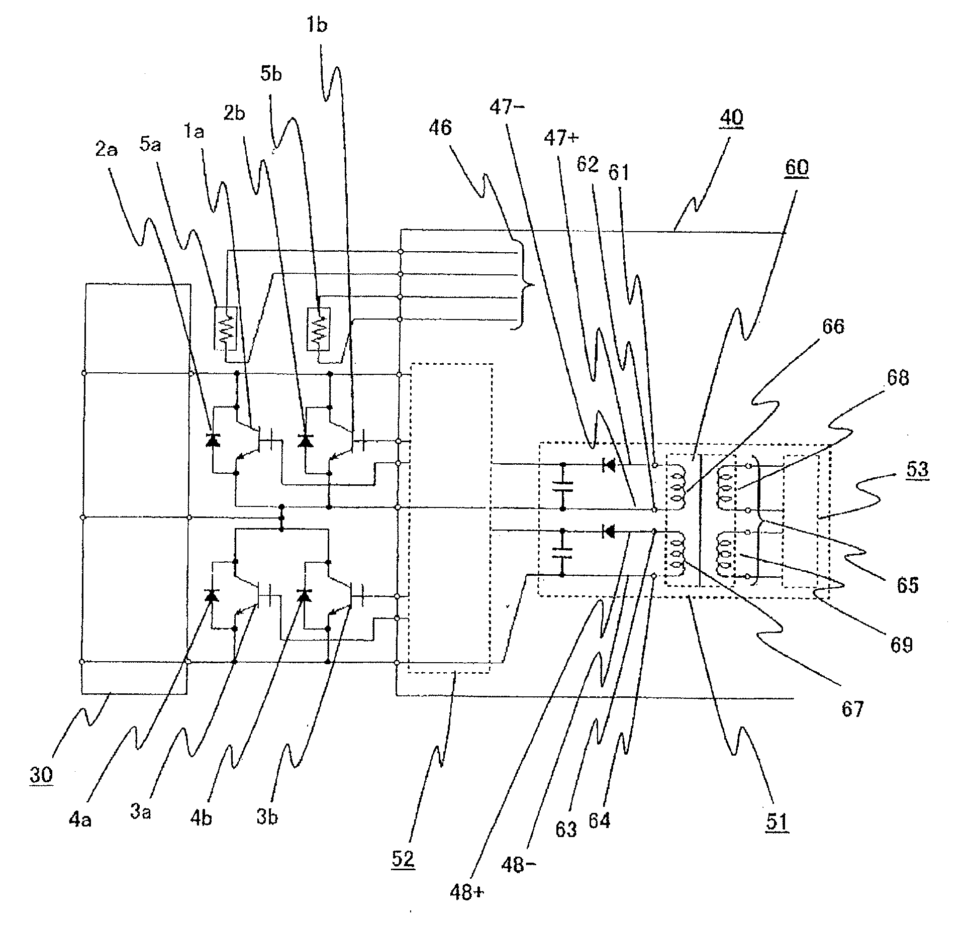
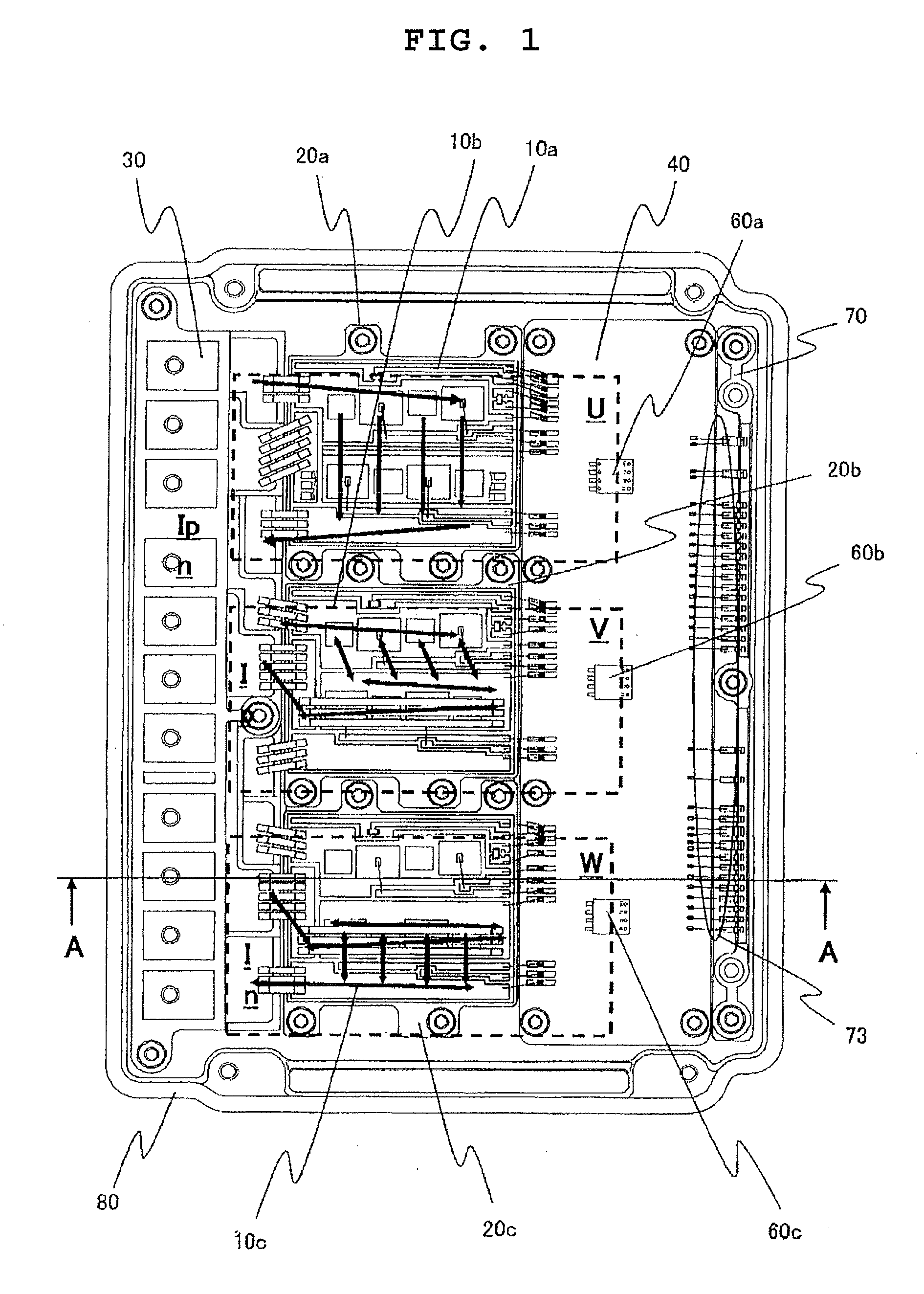
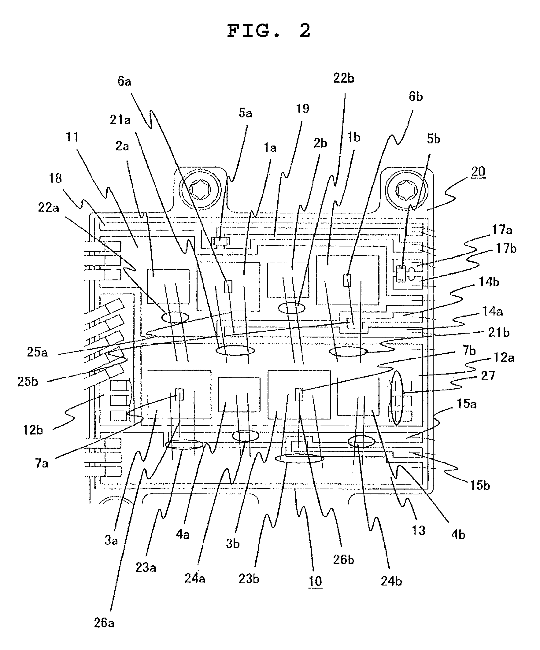
[0042]FIG. 1 illustrates a power converter according to an example of the invention. FIGS. 2 and 3 illustrate the details of an enlarged part shown in FIG. 1. In FIG. 2, emitter electrodes and upper arm gate electrodes 6a and 6b are provided on the upper surfaces of upper arm IGBT (insulated gate bipolar transistor) chips 1a and 1b, respectively, and collector electrodes are provided on the lower surfaces of the chips 1a and 1b. On the other hand, anode electrodes are provided on the upper surfaces of upper arm diode chips 2a and 2b, and cathode electrodes are provided on the lower surfaces of the chips 2a and 2b. Lower arm IGBT chips 3a and 3b, and lower arm diode chips 4a and 4b have terminals similar to the corresponding terminals of the upper arm.

[0043]The lower surfaces of the upper arm IGBT chips 1a and 1b and the upper arm diode chips 2a and 2b are brazed by solder or the like ont...

embodiment 2

[0090]FIG. 9 illustrates the details of an enlarged part of the insulating substrate 10 of a power converter according to this embodiment, corresponding to FIG. 2 in the embodiment 1. According to this embodiment, an upper gate return wiring pattern 212 is provided between the gate wiring pattern 14a and the alternating current wiring pattern 12a on the insulating substrate 10 substantially in parallel with the respective patterns 14a and 12a as illustrated in FIG. 10. The upper gate return wiring pattern 212 is connected with the emitter electrodes of the upper arm IGBT chips 1a and 1b via aluminum wires 221a and 221b. The upper gate return wiring pattern 212 is further connected with the terminal 50 of the alternating current pattern 43 via the aluminum wire 71. In this embodiment, therefore, the upper gate return wiring pattern 212 functions as a high potential side emitter wiring. On the other hand, the alternating current wiring pattern 12a functions as a low potential side col...

embodiment 3

[0094]FIG. 10 illustrates an example of the insulating substrate 10 which contains one chip for each type of chips in the power converter shown in FIGS. 1 through 7, corresponding to FIG. 2 in the embodiment 1. As illustrated in FIG. 12, the upper arm IGBT chip 1a, the upper arm diode chip 2a, the lower arm IGBT chip 3a, and the lower arm diode chip 4a are disposed one for each on the insulating substrate 10 in this embodiment. The gate electrode of the upper arm IGBT chip 1a is connected with the upper arm gate wiring pattern 14a, and the gate electrode of the lower arm IGBT chip 3a is connected with the lower arm gate wiring pattern 15a. The aluminum ribbon 72 is directly connected with the alternating current wiring pattern 12a. Other structures are similar to the corresponding structures shown in FIGS. 1 through 6, and provide similar effects. The structures in this embodiment can offer advantages similar to the advantages described above.


PUM


Abstract

A power converter which has a power module allowing supply and cutoff of main current, and a driver module controlling supply and cutoff of the main current allowed by the power module includes: a high potential side semiconductor device which allows supply and cutoff of the main current on the high potential side of the power module; a low potential side semiconductor device which allows supply and cutoff of the main current on the low potential side of the power module, and is connected with the high potential side semiconductor device in series; plural power module side wirings connected with respective electrodes contained in the high potential side semiconductor device and the low potential side semiconductor device, and disposed adjacent to each other substantially on the same plane as the power module in the order of applied potentials with a connection end between the plural power module side wirings and the driver module located along the end of the power module; plural driver module side wirings provided on the driver module as wirings connected with the plural corresponding power module side wirings, and disposed adjacent to each other substantially on the same plane as the driver module in the order corresponding to the positions of the plural power module side wirings in positions along the end of the driver module; a power source transformer as a circuit which converts a signal voltage for controlling the supply and cutoff of the main current by the driver module into voltage applied to a control electrode of the high potential side semiconductor device and a control electrode of the low potential side semiconductor device, plural terminals of the power source transformer in correspondence with the plural driver module side wirings being provided in the order of the positions of the plural corresponding driver module side wirings; and conductors disposed in the vicinity of the plane on which the plural power module side wirings are provided and in the vicinity of the plane on which the plural driver module side wirings are provided, and electrically connected in such positions as to surround magnetic flux generated by current looping at least through the power source transformer, the driver module side wirings, and the power module side wirings.

Description

TECHNICAL FIELD[0001]The present invention relates to a power converter, and more particularly to a power converter for a hybrid system of an automobile.BACKGROUND ART[0002]A power converter for a hybrid system of an automobile controls motor current by switching of a power semiconductor device. With increase in the output from the hybrid system in recent years, motor current and voltage of the system are increasing. Therefore, the problem of surge voltage generated at the time of switching of the power semiconductor device has been an issue to overcome.[0003]Conventionally, surge voltage generated by switching is decreased by reduction of main circuit inductances of the power semiconductor device and a capacitor achieved by shortening the wiring lengths of the power semiconductor device and the capacitor and laminating the wirings thereof, and laminating the wirings inside the capacitor, or by other methods (for example, see PTL 1). The reduction of surge voltage allows high-speed ...

Claims


Application Information

Patent Timeline
IPC IPC(8): H02M7/00
CPCH02M7/003H03K17/691H01L2224/49111H01L2924/1305H01L2924/13055H01L2924/00H02M3/00H01L2224/0603H01L2924/19107H01L2224/4903H01L2224/40137H01L2224/40139H01L2224/48227
Inventor FUJINO, SHINICHITAKAGI, YUSUKEHAKUTO, TAKUMA
Owner HITACHI ASTEMO LTD
Why Eureka
Try Eureka