Organic electroluminescent device

a technology of electroluminescent devices and organic materials, applied in thermoelectric devices, triarylamine dyes, luminescent compositions, etc., can solve the problems of high efficiency, low efficiency, and “roll-off” behaviour at high luminous densities, and achieve the effect of improving efficiency and/or lifetime, roll-off behaviour and/or processability

Active Publication Date: 2012-12-27
MERCK PATENT GMBH
View PDF2 Cites 65 Cited by
  • Summary
  • Abstract
  • Description
  • Claims
  • Application Information

AI Technical Summary

Benefits of technology

[0006]Surprisingly, it has been found that an organic electroluminescent device which comprises a mixture of at least two materials whose HOMO are at least 0.15 eV apart and at least one of which is a hole-transport material in at least one hole-transport layer exhibits significant improvements with respect to the efficiency and / or lifetime and / or roll-off behaviour and / or processability during device production.

Problems solved by technology

A further problem for which there is still a need for improvement is the so-called “roll-off” behaviour.
Thus, very high efficiency is obtained at very low luminous densities, while only low efficiency is obtained at high luminous densities, in particular in the case of phosphorescent OLEDs.
The very high efficiency at low luminous density is therefore undesired since this is accompanied by problems in the addressing of the OLED.
Thus, there are in some cases problems that the hole-transport materials in particular crystallise, for example on the shadow mask, during application, which makes device production significantly more difficult.
This is particularly problematic, in particular, during application of the hole-transport layer, since these layers are usually very thick, meaning that a lot of material is used here.
Crystallisation of the materials thus has particularly adverse effects here.

Method used


Image

  • Organic electroluminescent device
  • Organic electroluminescent device
  • Organic electroluminescent device

Examples


examples

Production of OLEDs

[0121]OLEDs according to the invention and OLEDs in accordance with the prior art are produced by a general process in accordance with WO 2004 / 058911, which is adapted to the circumstances described here (layer-thickness variation, materials used).

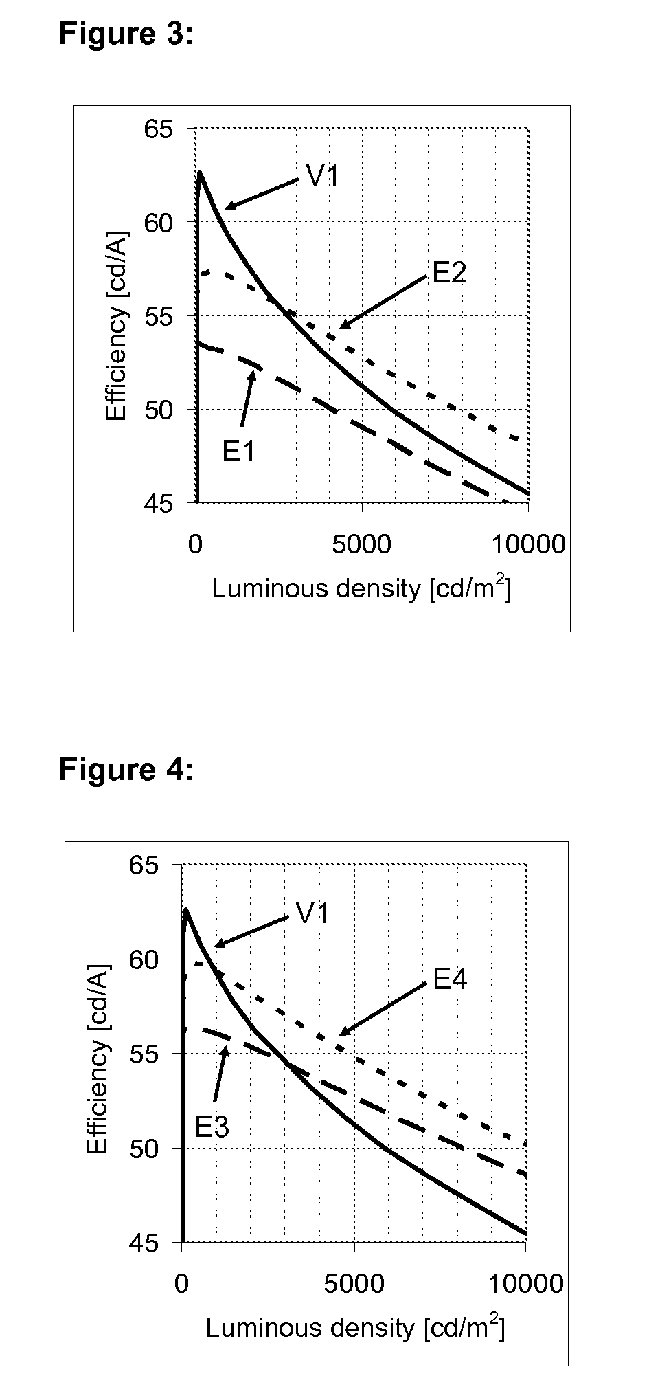
[0122]The data for various OLEDs are presented in Examples V1-E34 below (see Tables 1 and 2). Glass plates coated with structured ITO (indium tin oxide) in a thickness of 150 nm are coated with 20 nm of PEDOT (poly(3,4-ethylenedioxy-2,5-thiophene), applied by spin coating from water; purchased from H. C. Starck, Goslar, Germany) for improved processing.

[0123]These coated glass plates form the substrates to which the OLEDs are applied. The OLEDs have in principle the following layer structure: substrate / hole-injection layer (HIL) / optional interlayer (IL) / hole-transport layer (HTL) / emission layer (EML) / optional hole-blocking layer (HBL) / electron-transport layer (ETL) / optional electron-injection layer (EIL) and finally a ca...


PUM


Abstract

The present invention relates to organic electro-luminescent devices which in a hole transport layer have a mixture of two or more materials.

Description

CROSS-REFERENCE TO RELATED APPLICATIONS[0001]This application is a national stage application (under 35 U.S.C. §371) of PCT / EP2011 / 000500, filed Feb. 3, 2011, which claims benefit of German application 10 2010 010 481.7, filed Mar. 6, 2010.BACKGROUND OF THE INVENTION[0002]The present invention relates to organic electroluminescent devices which comprises a mixture of at least two materials, one of which is a hole-transport material, in at least one hole-transport layer.[0003]The structure of organic electroluminescent devices (OLEDs) in which organic semiconductors are employed as functional materials is described, for example, in U.S. Pat. No. 4,539,507, U.S. Pat. No. 5,151,629, EP 0676461 and WO 98 / 27136. However, there continues to be a need for improvement, in particular with respect to the efficiency and lifetime. A further problem for which there is still a need for improvement is the so-called “roll-off” behaviour. This is taken to mean that the efficiency of an organic elect...

Claims


Application Information

Patent Timeline
Patent Type & Authority Applications(United States)
IPC IPC(8): H01L51/54H01L51/56
CPCC09K11/06H01L51/0059H01L51/5004H01L51/5052C09B57/10C09B57/00C09B57/007C09B57/008H05B33/22H10K85/631H10K50/11H10K2101/40H10K50/165H10K50/155
Inventor PFLUMM, CHRISTOFVOGES, FRANKANÉMIAN, RÉMI MANOUK
Owner MERCK PATENT GMBH
Why Eureka
Try Eureka