Light emitting diode element, method of fabrication and light emitting device
- Summary
- Abstract
- Description
- Claims
- Application Information
AI Technical Summary
Problems solved by technology
Method used
Image

Examples
Embodiment Construction
[0030]The technical contents, detailed explanation and effect of the present invention may be further understood with reference to the following description and the appended drawings.
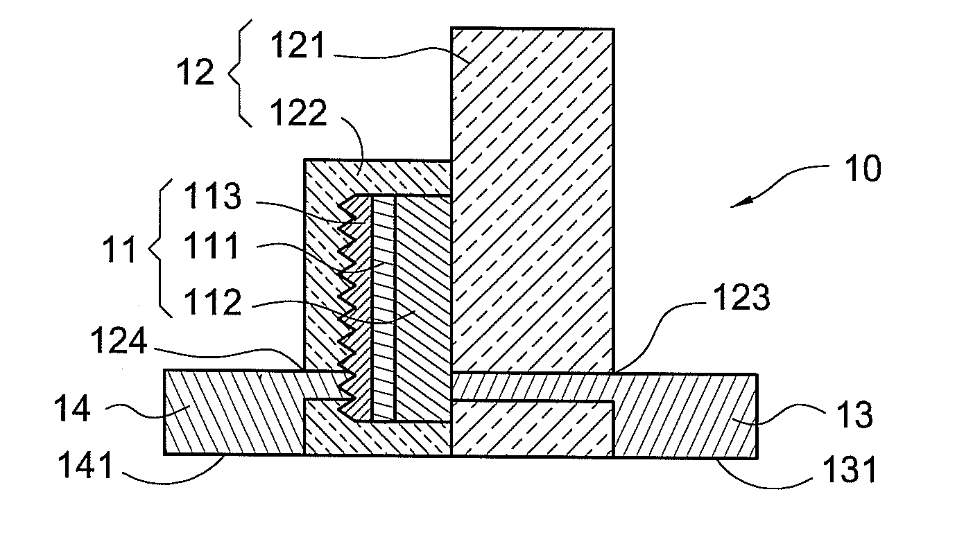
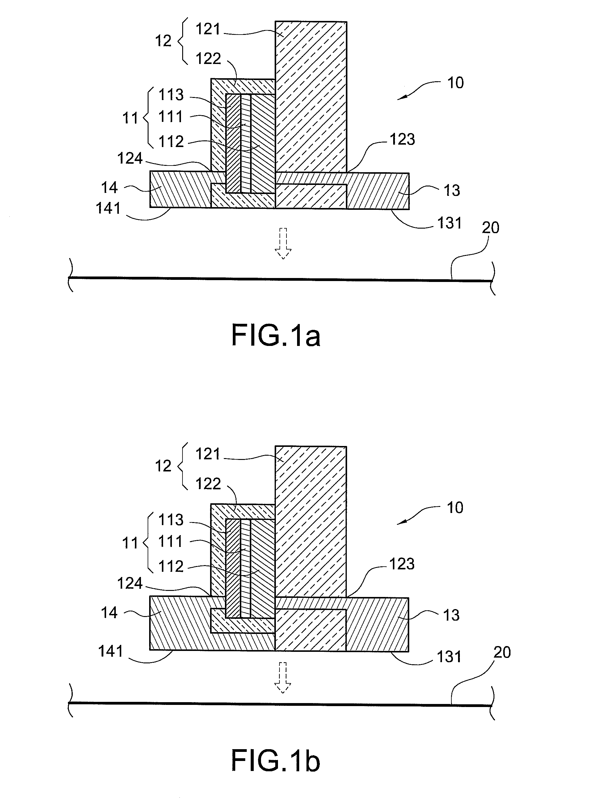
[0031]Please refer to FIG. 1a, which shows a sectional view of a first preferred example of an LED element according to the invention. The LED element 10 is used for mounting on a predetermined surface 20. The predetermined surface 20 may be a base or a mounting surface of a printed circuit board (PCB). The LED element 10 may self-stand on the predetermined surface 20. As shown in FIG. 1a, the LED element 10 mainly comprises a multi-layer semiconductor 11, a light transmissive substrate 121, a light transmissive insulator 122, a first electrode 13 and a second electrode 14.
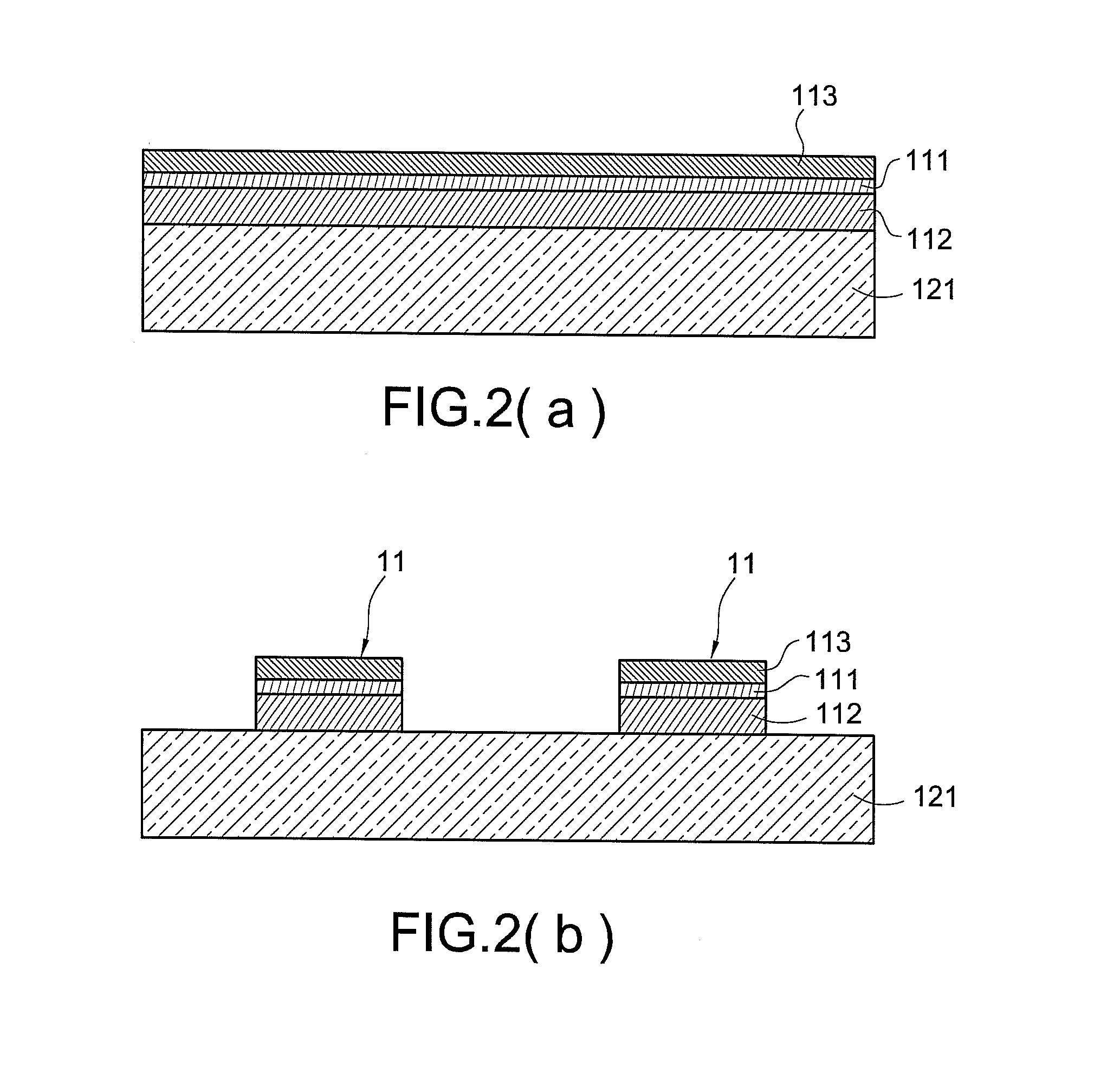
[0032]The multi-layer semiconductor 11 has a light emitting active layer 111 substantially perpendicular to the predetermined surface 20, a first semiconductor layer 112 located on a surface of the light emitting active layer 111 and ...
PUM
 Abstract
Description
Claims
Application Information
 - R&D Engineer
- R&D Manager
- IP Professional
- Industry Leading Data Capabilities
- Powerful AI technology
- Patent DNA Extraction
Browse by: Latest US Patents, China's latest patents, Technical Efficacy Thesaurus, Application Domain, Technology Topic.
© 2024 PatSnap. All rights reserved.Legal|Privacy policy|Modern Slavery Act Transparency Statement|Sitemap